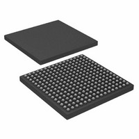
AD6636CBCZ Analog Devices Inc, AD6636CBCZ Datasheet - Page 21

AD6636CBCZ
Manufacturer Part Number
AD6636CBCZ
Description
IC DIGITAL DWNCONV 4CH 256CSPBGA
Manufacturer
Analog Devices Inc
Series
AD6636r
Datasheet
1.AD6636BCPCB.pdf
(80 pages)
Specifications of AD6636CBCZ
Rf Type
Cellular, CDMA2000, EDGE, GPRS, GSM
Number Of Mixers
1
Secondary Attributes
Down Converter
Current - Supply
450mA
Voltage - Supply
3 V ~ 3.6 V
Package / Case
256-CSPBGA
Brief Features
4/6 Independent Wideband Processing Channel, Quadrature Correction & DC Correction For Complex Input
Supply Voltage Range
1.7V To 1.9V
Operating Temperature Range
-40°C To +85°C
Ic Function
Digital Down Converter (DDC)
Rohs Compliant
Yes
Pin Count
256
Screening Level
Industrial
Package Type
CSPBGA
Lead Free Status / RoHS Status
Lead free / RoHS Compliant
Frequency
-
Gain
-
Noise Figure
-
Lead Free Status / Rohs Status
Compliant
Available stocks
Company
Part Number
Manufacturer
Quantity
Price
Company:
Part Number:
AD6636CBCZ
Manufacturer:
ADI
Quantity:
240
Scaling with Floating-Point ADC
An example of the exponent control feature combines the
AD6600 and the AD6636. The AD6600 is an 11-bit ADC with
three bits of gain ranging. In effect, the 11-bit ADC provides the
mantissa, and the three bits of the relative signal strength
indicator (RSSI) are the exponent. Only five of the eight
available steps are used by the AD6600. See the AD6600 data
sheet for details.
Table 10. Weighting Factors for Different Exp[2:0] Values
ADC Input
Level
Largest
Smallest
Complex (I/Q) Input Ports
The four individual ADC input ports of the AD6636 can be
configured to function as two complex input ports.
Additionally, if required, only two input ports can be made to
function as a complex port, while the remaining two input ports
function as real individual input ports.
In complex mode, Input Port A is paired with Input Port B to
receive I and Q data, respectively. Similarly, Input Port C can be
paired with Input Port D to receive I and Q data, respectively.
These two pairings are controlled individually using Bit 24 and
Bit 25 of the ADC input control register.
As explained previously, each individual channel can receive
input signals from any of the four input ports using the crossbar
mux select bits in the ADC input control register. In addition to
the three bits, a 1-bit selection is provided for choosing the
complex input port option for any individual channel. For
example, if Channel 0 needs to receive complex input from
Input Port A and Input Port B, the mux select bits should
Figure 23. Typical Interconnection of the AD6645 Fixed-Point ADC and AD6636
GAIN RANGING CONTROL
AD6636
Exp[2:0]
000 (0)
001 (1)
010 (2)
011 (3)
100 (4)
101 (5)
110 (6)
111 (7)
BITS OR GROUNDED
14-BIT ADC
AD6645
EXPONENT BITS
D13 (MSB)
D0 (LSB)
Data
Divide-By
/1 (>> 0)
/2 (>> 1)
/4 (>> 2)
/8 (>> 3)
/16 (>> 4)
/32 (>> 5)
/64 (>> 6)
/128 (>> 7)
IN15
IN2
IN1
IN0
EXP2
EXP1
EXP0
AD6636
Signal
Attenuation (dB)
0
6
12
18
24
30
36
42
Rev. A | Page 21 of 80
indicate Input Port A, and the complex input bit should be
selected.
When the input ports are paired for complex input operation,
only one set of exponent bits is driven externally with gain
control output. Therefore, when Input Port A and Input Port B
form a complex input, EXPA[2:0] are output and, similarly, for
Input Port C and Input Port D, EXPC[2:0] are output.
LVDS Input Ports
The AD6636 input ports can be configured in CMOS mode or
LVDS mode. In CMOS input mode, the four input ports can be
configured as two complex input ports. In LVDS mode, two CMOS
input ports are each combined to form one LVDS input port.
CMOS Input Port INA[15:0] and CMOS Input Port INB[15:0]
form the positive and negative differential nodes,
LVDS_A+[15:0] and LVDS_A−[15:0], respectively. Similarly,
INC[15:0] and IND[15:0] form the positive and negative
differential nodes, LVDS_C+[15:0] and LVDS_C− [15:0],
respectively. CLKA and CLKB form the differential pair,
Pin LVDS_CLKA+ and Pin LVDS_CLKA−. Similarly, CLKC
and CLKD form the differential pair Pin LVDS_CLKC+ and
Pin LVDS_CLKC−.
By default, the AD6636 powers up in CMOS mode and can be
programmed to CMOS mode by using the CMOS mode bit
(Bit 10 of the LVDS control register). Writing Logic 1 to Bit 8 of
the LVDS control register enables an autocalibrate routine that
calibrates the impedance of the LVDS pads to match the output
impedance of the LVDS signal source impedance. The LVDS pads
in the AD6636 have an internal impedance of 100 Ω across the
differential signals; therefore, an external resistor is not required.
PLL CLOCK MULTIPLIER
In the AD6636, the input clock rate must be the same as the
input data rate. In a typical digital downconverter architecture,
the clock rate is a limitation on the number of filter taps that
can be calculated in the programmable RAM coefficient filters
(MRCF, DRCF, and CRCF). For slower ADC clock rates (or for
any clock rate), this limitation can be overcome by using a PLL
clock multiplier to provide a higher clock rate to the RCF filters.
Using this clock multiplier, the internal signal processing clock
rate can be increased up to 200 MHz. The CLKA signal is used
as an input to the PLL clock multiplier.
CLKA
PLL CLOCK GENERATION
(1, 2, 4 OR 8)
DIVIDE BY N
N
2
Figure 24. PLL Clock Generation
PLL CLOCK
MULITPLIER
(4x TO 20x)
M
5
BYPASS_PLL
1 FOR BYPASS
1
0
0
1
ADC_CLK
PLL_CLK
AD6636


