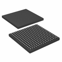
AD6636CBCZ Analog Devices Inc, AD6636CBCZ Datasheet - Page 13

AD6636CBCZ
Manufacturer Part Number
AD6636CBCZ
Description
IC DIGITAL DWNCONV 4CH 256CSPBGA
Manufacturer
Analog Devices Inc
Series
AD6636r
Datasheet
1.AD6636BCPCB.pdf
(80 pages)
Specifications of AD6636CBCZ
Rf Type
Cellular, CDMA2000, EDGE, GPRS, GSM
Number Of Mixers
1
Secondary Attributes
Down Converter
Current - Supply
450mA
Voltage - Supply
3 V ~ 3.6 V
Package / Case
256-CSPBGA
Brief Features
4/6 Independent Wideband Processing Channel, Quadrature Correction & DC Correction For Complex Input
Supply Voltage Range
1.7V To 1.9V
Operating Temperature Range
-40°C To +85°C
Ic Function
Digital Down Converter (DDC)
Rohs Compliant
Yes
Pin Count
256
Screening Level
Industrial
Package Type
CSPBGA
Lead Free Status / RoHS Status
Lead free / RoHS Compliant
Frequency
-
Gain
-
Noise Figure
-
Lead Free Status / Rohs Status
Compliant
Available stocks
Company
Part Number
Manufacturer
Quantity
Price
Company:
Part Number:
AD6636CBCZ
Manufacturer:
ADI
Quantity:
240
Mnemonic
SERIAL PORT CONTROL
SCLK
SDO
SDI
STFS
SRFS
SCS
MSB_FIRST
SMODE
JTAG
TRST
TCLK
TMS
TDO
TDI
1
2
PIN LISTING FOR POWER, GROUND, DATA, AND ADDRESS BUSES
Table 9.
Mnemonic
VDDCORE
VDDIO
GND
INA[0:15]
INB[0:15]
INC[0:15]
IND[0:15]
PA[0:15]
PB[0:15]
PC[0:15]
D[0:15]
A[0:7]
Pin with a pull-up resistor of nominal 70 kΩ.
Pin with a pull-down resistor of nominal 70 kΩ.
1
2
1
1
1
2
Type
Input
Output
Input
Input
Input
Input
Input
Input
Input
Input
Input
Output
Input
Pin No.
A9, G6, G11, H1, H6, H11, J6, J11, J16, K6, K11, T8
B2, B15, F7, F8, F9, F10, L7, L8, L9, L10, R2, R15
A1, A8, A16, E5, F6, F11, G7, G8, G9, G10, H7, H8, H9, H10, H16, J1, J7, J8, J9, J10, K7, K8, K9, K10, L6, L11,
M5, P7, T1, T9, T10, T15, T16
N3, P2, P1, N2, N1, M1, L2, K3, K2, J2, H2, G1, F1, F2, E1, E2
M4, L4, M3, L5, L3, M2, K4, K5, J4, J5, J3, H4, H3, G2, H5, G3
C3, C4, B3, A2, D6, C6, E7, D7, E8, D8, C8, E9, D9, C9, B10, E10
B1, E6, D5, C5, A3, B4, B5, A4, B6, C7, B7, A7, B8, B9, A10, A11
F16, H15, G16, J12, J15, J14, K16, J13, K15, K14, L16, M16, K12, L15, N16, K13
F13, E15, G14, G12, E13, E14, F12, F14, C14, D14, C16, A15, B16, D15, D13, C15
M14, N14, M13, L12, P14, N13, R14, M12, T14, R13, P13, P12, M11, T13, T12, N12
R10, N9, N8, T7, P9, M9, R9, T5, T6, P8, R7, R8, N7, M7, R6, M8
N11, R12, P11, R11, N10, M10, P10, T11
Pin No.
R1
M6
N11
N4
P4
N5
P5
B13
C12
C11
A13
D10
R3
Function
Serial Clock.
Serial Port Data Output (Open drain output, needs external pull-up resistor 1KΩ).
Serial Port Data Input.
Serial Transmit Frame Sync.
Serial Receive Frame Sync.
Serial Chip Select.
Select MSB First into SDI Pin and MSB First Out of SDO Pin.
Logic 0 = MSB first; Logic 1 = LSB first.
Serial Mode Select. Pull high when serial port is used and low when microport is used.
Test Reset Pin. Pull low when JTAG is not used.
Test Clock.
Test Mode Select.
Test Data Output. Three-stated when JTAG is in reset.
Test Data Input.
Rev. A | Page 13 of 80
AD6636


