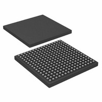
AD6636CBCZ Analog Devices Inc, AD6636CBCZ Datasheet - Page 20

AD6636CBCZ
Manufacturer Part Number
AD6636CBCZ
Description
IC DIGITAL DWNCONV 4CH 256CSPBGA
Manufacturer
Analog Devices Inc
Series
AD6636r
Datasheet
1.AD6636BCPCB.pdf
(80 pages)
Specifications of AD6636CBCZ
Rf Type
Cellular, CDMA2000, EDGE, GPRS, GSM
Number Of Mixers
1
Secondary Attributes
Down Converter
Current - Supply
450mA
Voltage - Supply
3 V ~ 3.6 V
Package / Case
256-CSPBGA
Brief Features
4/6 Independent Wideband Processing Channel, Quadrature Correction & DC Correction For Complex Input
Supply Voltage Range
1.7V To 1.9V
Operating Temperature Range
-40°C To +85°C
Ic Function
Digital Down Converter (DDC)
Rohs Compliant
Yes
Pin Count
256
Screening Level
Industrial
Package Type
CSPBGA
Lead Free Status / RoHS Status
Lead free / RoHS Compliant
Frequency
-
Gain
-
Noise Figure
-
Lead Free Status / Rohs Status
Compliant
Available stocks
Company
Part Number
Manufacturer
Quantity
Price
Company:
Part Number:
AD6636CBCZ
Manufacturer:
ADI
Quantity:
240
AD6636
THEORY OF OPERATION
ADC INPUT PORT
The AD6636 features four identical, independent high speed
ADC input ports named A, B, C, and D. These input ports have
the flexibility to allow independent inputs, diversity inputs, or
complex I/Q inputs. Any of the ADC input ports can be routed
to any of the six tuner channels; that is, any of the six. The
AD6636 channels can receive input data from any of the input
ports. Time-multiplexed inputs on a single port are not
supported in the AD6636.
These four input ports can operate at up to 150 MSPS. Each
input port has its own clock (CLKA, CLKB, CLKC, and CLKD)
used for registering input data into the AD6636. To allow slow
input rates while providing fast processing clock rates, the
AD6636 contains an internal PLL clock multiplier that supplies
the internal signal processing clock. CLKA is used as an input
to the PLL clock multiplier. Additional programmability allows
the input data to be clocked into the part either on the rising
edge or the falling edge of the input clock.
In addition, the front end of the AD6636 contains circuitry that
enables high speed signal-level detection, gain control, and
quadrature I/Q correction. This is accomplished with a unique
high speed level-detection circuit that offers minimal latency
and maximum flexibility to control all four input signals
(typically ADC inputs) individually. The input ports also
provide input power-monitoring functions via various modes
and magnitude and phase I/Q correction blocks. See the
Quadrature I/Q Correction Block section for details.
Each individual processing channel can receive input data from
any of the four input ports individually. This is controlled using
3-bit crossbar mux-select bit words in the ADC input control
register. Each individual channel has a similar 3-bit selection. In
addition to the four input ports, an internal test signal (PN—
pseudorandom noise sequence) can also be selected. This
internal test signal is discussed in the User-Configurable, Built-
In Self-Test (BIST) section.
Input Data Format
Each input port consists of a 16-bit mantissa and a 3-bit
exponent (16 + 3 floating-point input, or up to 16-bit fixed-
point input). When interfacing to standard fixed-point ADCs,
the exponent bit should either be connected to ground or be
programmed as outputs for gain control output. If connected to
a floating-point ADC (also called gain ranging ADC), the
exponent bits from the ADC can be connected to the input
exponent bits of the AD6636. The mantissa data format is twos
complement, and the exponent is unsigned binary.
Rev. A | Page 20 of 80
The 3-exponent bits are shared with the gain range control bits
in the hardware. When floating-point ADCs are not used, these
three pins on each ADC input port can be used as gain range
control output bits.
Input Timing
The data from each high speed input port is latched either on
the rising edge or the falling edge of the port’s individual CLKx
(where x stands for A, B, C, or D input ports). The ADC clock
invert bit in ADC clock control register selects the edge of the
clock (rising or falling) used to register input data into the
AD6636.
The clock signals (CLKA, CLKB, CLKC, and CLKD) can
operate at up to 150 MHz. In applications using high speed
ADCs, the ADC sample clock, data valid, or data-ready strobe
are typically used to clock the AD6636.
Connection to Fixed-Point ADC
For fixed-point ADCs, the AD6636 exponent inputs, EXP[2:0],
are not typically used and should be tied low. Alternatively,
because these pins are shared with gain range control bits, if the
gain ranging block is used, these pins can be used as outputs of
the gain range control block. The ADC outputs are tied directly
to the AD6636 inputs, MSB justified. Therefore, for fixed-point
ADCs, the exponents are typically static and no input scaling is
used in the AD6636. Figure 23 shows a typical interconnection.
EXPx [2:0]
EXPx [2:0]
INx [15:0]
INx [15:0]
CLKx
CLKx
(Falling Edge of Clock, x = A, B, C, or D for Four Input Ports)
(Rising Edge of Clock, x = A, B, C, or D for Four Input Ports)
Figure 21. Input Data Timing Requirements
Figure 22. Input Data Timing Requirements
t
t
SI
SI
DATA n
DATA n
t
t
HI
HI
DATA n + 1
DATA n + 1


