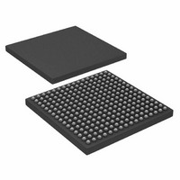
AD6636CBCZ Analog Devices Inc, AD6636CBCZ Datasheet - Page 71

AD6636CBCZ
Manufacturer Part Number
AD6636CBCZ
Description
IC DIGITAL DWNCONV 4CH 256CSPBGA
Manufacturer
Analog Devices Inc
Series
AD6636r
Datasheet
1.AD6636BCPCB.pdf
(80 pages)
Specifications of AD6636CBCZ
Rf Type
Cellular, CDMA2000, EDGE, GPRS, GSM
Number Of Mixers
1
Secondary Attributes
Down Converter
Current - Supply
450mA
Voltage - Supply
3 V ~ 3.6 V
Package / Case
256-CSPBGA
Brief Features
4/6 Independent Wideband Processing Channel, Quadrature Correction & DC Correction For Complex Input
Supply Voltage Range
1.7V To 1.9V
Operating Temperature Range
-40°C To +85°C
Ic Function
Digital Down Converter (DDC)
Rohs Compliant
Yes
Pin Count
256
Screening Level
Industrial
Package Type
CSPBGA
Lead Free Status / RoHS Status
Lead free / RoHS Compliant
Frequency
-
Gain
-
Noise Figure
-
Lead Free Status / Rohs Status
Compliant
Available stocks
Company
Part Number
Manufacturer
Quantity
Price
Company:
Part Number:
AD6636CBCZ
Manufacturer:
ADI
Quantity:
240
DRCF Taps <6:0>
This register is written with one less than the number of taps
that are calculated by the DRCF filter. The filter length is given
by the decimal value of this register plus 1. A value of 0
represents a 1-tap filter, and a value of 0x28 (40 decimal)
represents a 41-tap filter.
DRCF Start Address <5:0>
This register is written with the starting address of the DRCF
coefficient memory to be updated.
DRCF Final Address <5:0>
This register is written with the ending address of the DRCF
coefficient memory to be updated.
DRCF Coefficient Memory <13:0>
This memory consists of 64 words, and each word is 14 bits
wide. The data written to this memory space is expected to be
14-bit, twos complement format. See the Decimating RAM
Coefficient Filter (DRCF) section for the method to program
the coefficients into the coefficient memory.
CRCF Control Register <11:0>
<11>: CRCF Bypass Bit. When this bit is set, the DRCF filter is
bypassed and, therefore, its output is the same as its input.
When this bit is cleared, the CRCF has normal operation as
programmed by its control register.
<10>: Symmetry Bit. When this bit is set, it indicates that the
CRCF is implementing a symmetrical filter and only half the
impulse response needs to be written into the CRCF coefficient
RAM. When this bit is cleared, the filter is asymmetrical and
the complete impulse response of the filter should be written
into the coefficient RAM. When this filter is symmetrical, it can
implement up to 128 filter taps.
<9:8>: CRCF Multiply Accumulate Scale Bits. The output of the
CRCF filter is scaled according to the value of these bits.
Table 40 lists the attenuation corresponding to each setting.
Table 40. CRCF Multiply Accumulate Scale Bits
CRCF Scale<1:0>
00
01
10
11
<7:4>: CRCF Decimation Rate. This 4-bit word should be
written with one less than the decimation rate of the CRCF
filter. A value of 0 represents a decimation rate of 1 (no rate
change) and the maximum value of 15 represents a decimation
of 16. Filtering operation is done irrespective of the
decimation rate.
Scale Factor
18.06 dB attenuation (left-shift 3 bits)
12.04 dB attenuation (left-shift 2 bits)
6.02 dB attenuation (left-shift 1 bit)
No scaling (0 dB)
Rev. A | Page 71 of 80
<3:0>: CRCF Decimation Phase. This 4-bit word represents the
decimation phase used by the CRCF filter. The valid range is 0
to M
filter. This word is primarily used for synchronization of
multiple channels of the AD6636, when more than one channel
is used for filtering one signal (one carrier).
CRCF Coefficient Offset <5:0>
This register is used to specify which section of the 64-word
coefficient memory is used for a filter. It can be used to select
between multiple filters that are loaded into memory and
referenced by this pointer. This register is shadowed, and the
filter pointer is updated every time a new filter is started. This
allows the coefficient offset to be written even while a filter is
being computed without disturbing operation. The next sample
comes out of the CRCF with the new filter.
CRCF Taps <6:0>
This register is written with one less than the number of taps
that are calculated by the CRCF filter. The filter length is given
by the decimal value of this register plus 1. A value of 0
represents a 1-tap filter, and a value of 0x28 (40 decimal)
represents a 41-tap filter.
CRCF Coefficient Memory
This memory has 64 words that have 20 bits each. The memory
contains the CRCF filter coefficients. The data written to this
memory space is 20-bit in twos complement format. See the
Channel RAM Coefficient Filter section for the method to
program the coefficients into the coefficient memory.
AGC Control Register <10:0>
<10>: Channel Sync Select Bit. When this bit is set, the AGC
uses the sync signal from the channel for its synchronization.
When this bit is cleared, the SYNC pin used for synchronization
is defined by Bits <9:8> of this register.
<9:8>: SYNC Pin Select Bits. When Bit <10> of this register is
cleared, these bits specify the SYNC pin used by AGC for
synchronization. These bits are don’t care when Bit <10> of the
AGC control register is set to Logic 1.
Table 41. SYNC Pin Select Bits
AGC Control Bits <9:8>
00
01
10
11
CRCF
− 1, where M
CRCF
is the decimation rate of the CRCF
SYNC Pin Used by AGC
SYNC0
SYNC1
SYNC2
SYNC3
AD6636


