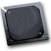
MPC564CZP40 Freescale Semiconductor, MPC564CZP40 Datasheet - Page 1033

MPC564CZP40
Manufacturer Part Number
MPC564CZP40
Description
IC MPU 32BIT W/CODE COMP 388PBGA
Manufacturer
Freescale Semiconductor
Series
MPC5xxr
Specifications of MPC564CZP40
Core Processor
PowerPC
Core Size
32-Bit
Speed
40MHz
Connectivity
CAN, EBI/EMI, SCI, SPI, UART/USART
Peripherals
POR, PWM, WDT
Number Of I /o
56
Program Memory Size
512KB (512K x 8)
Program Memory Type
FLASH
Ram Size
32K x 8
Voltage - Supply (vcc/vdd)
2.5 V ~ 2.7 V
Data Converters
A/D 32x10b
Oscillator Type
External
Operating Temperature
-40°C ~ 85°C
Package / Case
388-BGA
Processor Series
MPC5xx
Core
PowerPC
Data Bus Width
32 bit
Data Ram Size
32 KB
Interface Type
CAN, JTAG, QSPI, SCI, SPI, UART
Maximum Clock Frequency
40 MHz
Number Of Programmable I/os
56
Number Of Timers
2
Operating Supply Voltage
0 V to 5 V
Maximum Operating Temperature
+ 85 C
Mounting Style
SMD/SMT
Minimum Operating Temperature
- 40 C
On-chip Adc
2 (10 bit, 32 Channel)
For Use With
MPC564EVB - KIT EVAL FOR MPC561/562/563/564
Lead Free Status / RoHS Status
Contains lead / RoHS non-compliant
Eeprom Size
-
Lead Free Status / Rohs Status
No
Available stocks
Company
Part Number
Manufacturer
Quantity
Price
Company:
Part Number:
MPC564CZP40
Manufacturer:
Freescale Semiconductor
Quantity:
10 000
- Current page: 1033 of 1420
- Download datasheet (11Mb)
24.10.4.2 Read Operation
For a read access to internal READI registers, the following sequence of operations need to be performed
via the auxiliary port:
24.10.5 Error Handling
The READI module handles the various error conditions in the manner shown in the following sections.
24.10.5.1 Access Alignment
The READI module will force address alignment based on the word size field (SZ) value. If the SZ field
indicates word (32-bit) access, the least significant two bits of the read/write address field (RWAD) are
ignored. If the SZ field indicates half-word (16-bit) access, the least significant bit of the read/write address
field (RWAD) is ignored.
24.10.5.2 L-Bus Address Error
An address error occurs on the L-bus when the address phase of a cycle is not completed normally. This
could occur because of address not being valid or the address map not being valid. In such cases:
24.10.5.3 L-Bus Data Error
L-bus data error is signalled due to:
Freescale Semiconductor
2. The download request public message contains:
3. After the data has been written to the targeted register, the device ready for upload/download public
1. The tool confirms that the device is ready before transmitting upload request public message
2. The upload request public message contains:
3. The upload/download information public message (TCODE=19) is transmitted to the tool along
1. The access is terminated without retrying.
2. The SC bit of the RWA is reset. Block accesses do not continue.
3. The error message (TCODE = 8) is transmitted (error code 0b00011). Refer to
a) TCODE(18)
b) Access opcode, which specifies the register where data needs to be written, (e.g., access opcode
c) Data to be written to the register.
message (TCODE = 16) is transmitted to the tool indicating that the device is ready for next access.
(TCODE = 17).
a) TCODE(17)
b) Access opcode, which specifies the register where data needs to be read from, (for example,
with the data read from the targeted register indicating that the device is ready for next access.
0x14 indicates that DTA1 register is the target register).
access opcode 0x14 indicates that DTA1 register is the target register).
MPC561/MPC563 Reference Manual, Rev. 1.2
Table
24-20.
READI Module
24-65
Related parts for MPC564CZP40
Image
Part Number
Description
Manufacturer
Datasheet
Request
R

Part Number:
Description:
MPC5 1K0 5%
Manufacturer:
TE Connectivity
Datasheet:

Part Number:
Description:
MPC5 500R 5%
Manufacturer:
TE Connectivity
Datasheet:

Part Number:
Description:
MPC5 5K0 5%
Manufacturer:
Tyco Electronics
Datasheet:

Part Number:
Description:
MPC5 5R0 5%
Manufacturer:
Tyco Electronics
Datasheet:

Part Number:
Description:
MPC5 50K 5%
Manufacturer:
Tyco Electronics
Datasheet:

Part Number:
Description:
MPC5 1R0 5%
Manufacturer:
Tyco Electronics
Datasheet:
Part Number:
Description:
Manufacturer:
Freescale Semiconductor, Inc
Datasheet:
Part Number:
Description:
Manufacturer:
Freescale Semiconductor, Inc
Datasheet:
Part Number:
Description:
Manufacturer:
Freescale Semiconductor, Inc
Datasheet:
Part Number:
Description:
Manufacturer:
Freescale Semiconductor, Inc
Datasheet:
Part Number:
Description:
Manufacturer:
Freescale Semiconductor, Inc
Datasheet:


