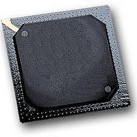
MPC564CZP40 Freescale Semiconductor, MPC564CZP40 Datasheet - Page 1036

MPC564CZP40
Manufacturer Part Number
MPC564CZP40
Description
IC MPU 32BIT W/CODE COMP 388PBGA
Manufacturer
Freescale Semiconductor
Series
MPC5xxr
Specifications of MPC564CZP40
Core Processor
PowerPC
Core Size
32-Bit
Speed
40MHz
Connectivity
CAN, EBI/EMI, SCI, SPI, UART/USART
Peripherals
POR, PWM, WDT
Number Of I /o
56
Program Memory Size
512KB (512K x 8)
Program Memory Type
FLASH
Ram Size
32K x 8
Voltage - Supply (vcc/vdd)
2.5 V ~ 2.7 V
Data Converters
A/D 32x10b
Oscillator Type
External
Operating Temperature
-40°C ~ 85°C
Package / Case
388-BGA
Processor Series
MPC5xx
Core
PowerPC
Data Bus Width
32 bit
Data Ram Size
32 KB
Interface Type
CAN, JTAG, QSPI, SCI, SPI, UART
Maximum Clock Frequency
40 MHz
Number Of Programmable I/os
56
Number Of Timers
2
Operating Supply Voltage
0 V to 5 V
Maximum Operating Temperature
+ 85 C
Mounting Style
SMD/SMT
Minimum Operating Temperature
- 40 C
On-chip Adc
2 (10 bit, 32 Channel)
For Use With
MPC564EVB - KIT EVAL FOR MPC561/562/563/564
Lead Free Status / RoHS Status
Contains lead / RoHS non-compliant
Eeprom Size
-
Lead Free Status / Rohs Status
No
Available stocks
Company
Part Number
Manufacturer
Quantity
Price
Company:
Part Number:
MPC564CZP40
Manufacturer:
Freescale Semiconductor
Quantity:
10 000
- Current page: 1036 of 1420
- Download datasheet (11Mb)
READI Module
the RWA register, and transmits the SC, RWAD, RW fields only is sufficient. This message will contain
41 bits instead of the 94 bits for writing the full contents of the RWA register. See
Section 24.6.4, “Partial Register
24.10.10 Throughput and Latency
Throughput analysis has been performed for various read/write access cases such as single write, block
write, single byte read, single word read, block byte read, block word read accesses to memory-mapped
locations. Data is presented for the two cases when the RWA register is written partially and completely.
24.10.10.1 Assumptions for Throughput Analysis
24-68
•
•
•
•
•
•
•
•
Single Write Access to memory-mapped
location – Word and Byte access
(In Million Messages Per Second)
Single Read Access to memory-mapped
location – Word access
(In Million Messages Per Second)
Single Read Access to memory-mapped
location – Byte access
(In Million Messages Per Second)
Block Write Access to memory-mapped
locations – 64-Kbyte block (Word and Byte) write
access
(In 64-Kbyte Block Writes Per Second)
All accesses are single read accesses only.
MCKI running at 28 MHz.
MCKO running at 56 MHz.
56-MHz internal operation.
Five clock internal L-bus access (read)
Output signals always free (not in middle of transmission) when requested.
One idle clock between read messages.
No delay from tool in responding — tool keeps up with READI port.
Table 24-31. Throughput Comparison for FPM and RPM MDO/MDI Configurations
The last data bit transmitted in the download request message (TCODE 18)
will always be the MSB of the register referenced by the opcode (SC field
in the case of the RWA register).
Access Type
Updates,” for RWAR and partial register update details respectively.
MPC561/MPC563 Reference Manual, Rev. 1.2
Full RWAR
NOTE
Update
Reduced Port Mode
2 MDO / 1 MDI pins
0.28
0.25
0.27
9
Partial RWAR
Update
0.35
0.51
0.56
9
Full RWAR
Update
0.53
0.52
0.53
8 MDO / 2 MDI pins
17
Full Port Mode
Table 24-11
Freescale Semiconductor
Partial RWAR
Update
0.65
1.05
1.05
17
and
Related parts for MPC564CZP40
Image
Part Number
Description
Manufacturer
Datasheet
Request
R

Part Number:
Description:
MPC5 1K0 5%
Manufacturer:
TE Connectivity
Datasheet:

Part Number:
Description:
MPC5 500R 5%
Manufacturer:
TE Connectivity
Datasheet:

Part Number:
Description:
MPC5 5K0 5%
Manufacturer:
Tyco Electronics
Datasheet:

Part Number:
Description:
MPC5 5R0 5%
Manufacturer:
Tyco Electronics
Datasheet:

Part Number:
Description:
MPC5 50K 5%
Manufacturer:
Tyco Electronics
Datasheet:

Part Number:
Description:
MPC5 1R0 5%
Manufacturer:
Tyco Electronics
Datasheet:
Part Number:
Description:
Manufacturer:
Freescale Semiconductor, Inc
Datasheet:
Part Number:
Description:
Manufacturer:
Freescale Semiconductor, Inc
Datasheet:
Part Number:
Description:
Manufacturer:
Freescale Semiconductor, Inc
Datasheet:
Part Number:
Description:
Manufacturer:
Freescale Semiconductor, Inc
Datasheet:
Part Number:
Description:
Manufacturer:
Freescale Semiconductor, Inc
Datasheet:


