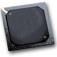
MPC564CZP40 Freescale Semiconductor, MPC564CZP40 Datasheet - Page 256

MPC564CZP40
Manufacturer Part Number
MPC564CZP40
Description
IC MPU 32BIT W/CODE COMP 388PBGA
Manufacturer
Freescale Semiconductor
Series
MPC5xxr
Specifications of MPC564CZP40
Core Processor
PowerPC
Core Size
32-Bit
Speed
40MHz
Connectivity
CAN, EBI/EMI, SCI, SPI, UART/USART
Peripherals
POR, PWM, WDT
Number Of I /o
56
Program Memory Size
512KB (512K x 8)
Program Memory Type
FLASH
Ram Size
32K x 8
Voltage - Supply (vcc/vdd)
2.5 V ~ 2.7 V
Data Converters
A/D 32x10b
Oscillator Type
External
Operating Temperature
-40°C ~ 85°C
Package / Case
388-BGA
Processor Series
MPC5xx
Core
PowerPC
Data Bus Width
32 bit
Data Ram Size
32 KB
Interface Type
CAN, JTAG, QSPI, SCI, SPI, UART
Maximum Clock Frequency
40 MHz
Number Of Programmable I/os
56
Number Of Timers
2
Operating Supply Voltage
0 V to 5 V
Maximum Operating Temperature
+ 85 C
Mounting Style
SMD/SMT
Minimum Operating Temperature
- 40 C
On-chip Adc
2 (10 bit, 32 Channel)
For Use With
MPC564EVB - KIT EVAL FOR MPC561/562/563/564
Lead Free Status / RoHS Status
Contains lead / RoHS non-compliant
Eeprom Size
-
Lead Free Status / Rohs Status
No
Available stocks
Company
Part Number
Manufacturer
Quantity
Price
Company:
Part Number:
MPC564CZP40
Manufacturer:
Freescale Semiconductor
Quantity:
10 000
- Current page: 256 of 1420
- Download datasheet (11Mb)
System Configuration and Protection
6.1.4.5
The interrupt overhead consists of two main parts:
The interrupt overhead can increase latency, and decrease the overall system performance. The overhead
of register saving time can be reduced by improving the operating system. The number of registers that
should be saved can be reduced if each interrupt event has its own interrupt vector. This solution solves
the interrupt source recognition overhead.
Only registers required for the recognition routine are considered to be saved in the calculations below.
Recognition of module internal events/channels is out of the scope of the calculations. See also the typical
interrupt handler flowchart in
6-16
•
•
Operation
Storage of general and special purpose registers
Recognition of the interrupt source
Details
Notes:
Total:
Interrupt Overhead Estimation for Enhanced Interrupt Controller Mode
Compiler and bus collision overhead are not included in the calculations.
If there is a need to enable
At Least 70-80 Clocks
Interrupt propagation from
request module to RCPU —
Store of some GPR and
SPR—10 clocks
Read SIPEND—4 clocks
Read SIMASK—4 clocks
SIPEND data processing —
20 clocks
(find first set, access to LUT in
the Flash, branches)
Read UIPEND—4 clocks
UIPEND data processing—20
clocks
(find first set, access to LUT in
the Flash, branches)
nesting of interrupts during
source recognition procedure,
at least 30 clocks should be
added to the interrupt latency
estimation
Architecture Without Using
8 clocks
Table 6-5. Interrupt Latency Estimation for Three Typical Cases
MPC561/MPC563
SIVEC
Figure
MPC561/MPC563 Reference Manual, Rev. 1.2
6-6.
Table 6-5
Interrupt propagation from
request module to RCPU —
Store of some GPR and SPR
—10 clocks
Read SIVEC—4 clocks
Branch to routine—10 clocks
Read UIPEND—4 clocks
UIPEND data processing —
(find first set, access to LUT in
the Flash, branches)
To use this feature in compressed
mode some undetermined
latency is added to make a
branch to compressed address of
the routine. This latency is
dependant on how the user code
is implemented.
At Least 50-60 Clocks
MPC561/MPC563 Architecture
8 clocks
20 clocks
NOTE
below illustrates the improvements.
Using SIVEC
Interrupt propagation from
request module to RCPU —
Store of some GPR and
SPR—10 clocks
Only one branch is executed to
reach the interrupt handler
routine of the device requesting
interrupt servicing—2 clocks
—
20 Clocks
6 clocks
Enhanced Interrupt
Controller Features
Architecture Using
MPC561/MPC563
Freescale Semiconductor
Related parts for MPC564CZP40
Image
Part Number
Description
Manufacturer
Datasheet
Request
R

Part Number:
Description:
MPC5 1K0 5%
Manufacturer:
TE Connectivity
Datasheet:

Part Number:
Description:
MPC5 500R 5%
Manufacturer:
TE Connectivity
Datasheet:

Part Number:
Description:
MPC5 5K0 5%
Manufacturer:
Tyco Electronics
Datasheet:

Part Number:
Description:
MPC5 5R0 5%
Manufacturer:
Tyco Electronics
Datasheet:

Part Number:
Description:
MPC5 50K 5%
Manufacturer:
Tyco Electronics
Datasheet:

Part Number:
Description:
MPC5 1R0 5%
Manufacturer:
Tyco Electronics
Datasheet:
Part Number:
Description:
Manufacturer:
Freescale Semiconductor, Inc
Datasheet:
Part Number:
Description:
Manufacturer:
Freescale Semiconductor, Inc
Datasheet:
Part Number:
Description:
Manufacturer:
Freescale Semiconductor, Inc
Datasheet:
Part Number:
Description:
Manufacturer:
Freescale Semiconductor, Inc
Datasheet:
Part Number:
Description:
Manufacturer:
Freescale Semiconductor, Inc
Datasheet:


