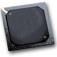
MPC564CZP40 Freescale Semiconductor, MPC564CZP40 Datasheet - Page 378

MPC564CZP40
Manufacturer Part Number
MPC564CZP40
Description
IC MPU 32BIT W/CODE COMP 388PBGA
Manufacturer
Freescale Semiconductor
Series
MPC5xxr
Specifications of MPC564CZP40
Core Processor
PowerPC
Core Size
32-Bit
Speed
40MHz
Connectivity
CAN, EBI/EMI, SCI, SPI, UART/USART
Peripherals
POR, PWM, WDT
Number Of I /o
56
Program Memory Size
512KB (512K x 8)
Program Memory Type
FLASH
Ram Size
32K x 8
Voltage - Supply (vcc/vdd)
2.5 V ~ 2.7 V
Data Converters
A/D 32x10b
Oscillator Type
External
Operating Temperature
-40°C ~ 85°C
Package / Case
388-BGA
Processor Series
MPC5xx
Core
PowerPC
Data Bus Width
32 bit
Data Ram Size
32 KB
Interface Type
CAN, JTAG, QSPI, SCI, SPI, UART
Maximum Clock Frequency
40 MHz
Number Of Programmable I/os
56
Number Of Timers
2
Operating Supply Voltage
0 V to 5 V
Maximum Operating Temperature
+ 85 C
Mounting Style
SMD/SMT
Minimum Operating Temperature
- 40 C
On-chip Adc
2 (10 bit, 32 Channel)
For Use With
MPC564EVB - KIT EVAL FOR MPC561/562/563/564
Lead Free Status / RoHS Status
Contains lead / RoHS non-compliant
Eeprom Size
-
Lead Free Status / Rohs Status
No
Available stocks
Company
Part Number
Manufacturer
Quantity
Price
Company:
Part Number:
MPC564CZP40
Manufacturer:
Freescale Semiconductor
Quantity:
10 000
- Current page: 378 of 1420
- Download datasheet (11Mb)
External Bus Interface
9.5.8.5
The transfer size signals (TSIZ[0:1]) indicate the size of the requested data transfer. During each transfer,
the TSIZ signals indicate how many bytes are remaining to be transferred by the transaction. The TSIZ
signals can be used with BURST and ADDR[30:31] to determine which byte lanes of the data bus are
involved in the transfer. For non-burst transfers, the TSIZ signals specify the number of bytes starting from
the byte location addressed by ADDR[30:31]. In burst transfers, the value of TSIZ is always 00.
9.5.8.6
The address type (AT[0:3]), program trace (PTR), and reservation transfer (RSV) signals are outputs that
indicate one of 16 address types. These types are designated as either a normal or alternate master cycle,
user or supervisor, and instruction or data type. The address type signals are valid at the rising edge of the
clock in which the special transfer start (STS) signal is asserted.
A special use of the PTR and RSV signals is for the reservation protocol described in
“Storage
cycles.
Table 9-7
by combining these pins.
9-38
ADDR[28:29]
Reservation.” Refer to
Address
Starting
summarizes the pins used to define the address type.
00
01
10
11
Transfer Size
Address Types
word 1 → word 2 → word 3
Burst Order (Assuming
word 0 → word 1 →
32-bit Port Size)
word 2 → word 3
word 2 → word 3
Asserted
word 3
Negated
Negated
Negated
Negated
BURST
Table 9-5. 4 Word Burst Length and Order
Section 9.5.14, “Show Cycle
MPC561/MPC563 Reference Manual, Rev. 1.2
Table 9-6. BURST/TSIZE Encoding
TSIZ[0:1]
Burst Length in
Words (Beats)
01
10
11
00
00
4
3
2
1
Burst (16 or 32 bytes)
Burst Length
Transfer Size
Transactions” for information on show
Table 9-8
Half-word
in Bytes
Word
Byte
16
12
8
4
x
lists all the definitions achieved
BDIP never asserted
Comments
Freescale Semiconductor
Section 9.5.10,
Related parts for MPC564CZP40
Image
Part Number
Description
Manufacturer
Datasheet
Request
R

Part Number:
Description:
MPC5 1K0 5%
Manufacturer:
TE Connectivity
Datasheet:

Part Number:
Description:
MPC5 500R 5%
Manufacturer:
TE Connectivity
Datasheet:

Part Number:
Description:
MPC5 5K0 5%
Manufacturer:
Tyco Electronics
Datasheet:

Part Number:
Description:
MPC5 5R0 5%
Manufacturer:
Tyco Electronics
Datasheet:

Part Number:
Description:
MPC5 50K 5%
Manufacturer:
Tyco Electronics
Datasheet:

Part Number:
Description:
MPC5 1R0 5%
Manufacturer:
Tyco Electronics
Datasheet:
Part Number:
Description:
Manufacturer:
Freescale Semiconductor, Inc
Datasheet:
Part Number:
Description:
Manufacturer:
Freescale Semiconductor, Inc
Datasheet:
Part Number:
Description:
Manufacturer:
Freescale Semiconductor, Inc
Datasheet:
Part Number:
Description:
Manufacturer:
Freescale Semiconductor, Inc
Datasheet:
Part Number:
Description:
Manufacturer:
Freescale Semiconductor, Inc
Datasheet:


