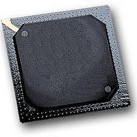
MPC564CZP40 Freescale Semiconductor, MPC564CZP40 Datasheet - Page 467

MPC564CZP40
Manufacturer Part Number
MPC564CZP40
Description
IC MPU 32BIT W/CODE COMP 388PBGA
Manufacturer
Freescale Semiconductor
Series
MPC5xxr
Specifications of MPC564CZP40
Core Processor
PowerPC
Core Size
32-Bit
Speed
40MHz
Connectivity
CAN, EBI/EMI, SCI, SPI, UART/USART
Peripherals
POR, PWM, WDT
Number Of I /o
56
Program Memory Size
512KB (512K x 8)
Program Memory Type
FLASH
Ram Size
32K x 8
Voltage - Supply (vcc/vdd)
2.5 V ~ 2.7 V
Data Converters
A/D 32x10b
Oscillator Type
External
Operating Temperature
-40°C ~ 85°C
Package / Case
388-BGA
Processor Series
MPC5xx
Core
PowerPC
Data Bus Width
32 bit
Data Ram Size
32 KB
Interface Type
CAN, JTAG, QSPI, SCI, SPI, UART
Maximum Clock Frequency
40 MHz
Number Of Programmable I/os
56
Number Of Timers
2
Operating Supply Voltage
0 V to 5 V
Maximum Operating Temperature
+ 85 C
Mounting Style
SMD/SMT
Minimum Operating Temperature
- 40 C
On-chip Adc
2 (10 bit, 32 Channel)
For Use With
MPC564EVB - KIT EVAL FOR MPC561/562/563/564
Lead Free Status / RoHS Status
Contains lead / RoHS non-compliant
Eeprom Size
-
Lead Free Status / Rohs Status
No
Available stocks
Company
Part Number
Manufacturer
Quantity
Price
Company:
Part Number:
MPC564CZP40
Manufacturer:
Freescale Semiconductor
Quantity:
10 000
- Current page: 467 of 1420
- Download datasheet (11Mb)
1
0x30 4800 STOP FRZ
0x30 4802
0x30 4804
0x30 4806
0x30 4808
0x30 480A
0x30 480C
0x30 480E
0x30 4810
0x30 4812
0x30 4814-
0x30 49FF
0x30
4A00-
0x30 4A7F
0x30
4A80-
0x30 4AFF
0x30
4B00-
0x30 4B7F
0x30 4B80
0x30 4BFF
13.2.2
The QADC64E occupies 1 Kbyte, or 512 16-bit entries, of address space. Ten 16-bit registers are control,
port, and status registers, 64 16-bit entries are the CCW table, and 64 16-bit entries are the result table, and
occupy 192 16-bit address locations because the result data is readable in three data alignment formats.
Each QADC64E module on the MPC561/MPC563 has its own memory space.
memory map for QADC64E module A, it occupies 0x30 4800 to 0x30 4BFF.
memory map for module B. Module B has the same offset scheme starting at 0x30 4C00. QADC64E B
occupies 0x30 4C00 to 0x30 4FFF.
Freescale Semiconductor
Address
Registers are accessible only as supervisor data space
Z
SIGN
EMU
CIE1
CIE2
CF1
MSB
Memory Map
X
0
TEST MODE
PF1 CF2 PF2 TOR
PIE
PIE
1
2
1
IRL1
SSE
SSE
0000 00
1
2
2
UNSIGNED LEFT JUSTIFIED
TR
PORTQA
G
DDRQA
3
SIGNED LEFT JUSTIFIED
MPC561/MPC563 Reference Manual, Rev. 1.2
Table 13-1. QADC64E_A Address Map
1
4
CWPQ1
MQ1
MQ2
TOR
5
2
LOC
K
P
6
IRL2
FLI
BY
P
P
7
QS
UNSIGNED RIGHT JUSTIFIED
RESUM
SUPV
E
8
IST
PSH
9
10
PORTQB
11
PSA
BQ2
CWPQ2
00 0000
00 0000
12
CHAN
CWP
QADC64E Legacy Mode Operation
Table 13-2
Table 13-1
13
PSL
14
LSB
15
displays the
shows the
Port Direction
Port Data
Reserved
Interrupt
Control 0
Control 1
Control 2
Register
Status 0
Status 1
Config.
Module
Results
Results
Results
CCWs
Test
1
1
13-3
1
Related parts for MPC564CZP40
Image
Part Number
Description
Manufacturer
Datasheet
Request
R

Part Number:
Description:
MPC5 1K0 5%
Manufacturer:
TE Connectivity
Datasheet:

Part Number:
Description:
MPC5 500R 5%
Manufacturer:
TE Connectivity
Datasheet:

Part Number:
Description:
MPC5 5K0 5%
Manufacturer:
Tyco Electronics
Datasheet:

Part Number:
Description:
MPC5 5R0 5%
Manufacturer:
Tyco Electronics
Datasheet:

Part Number:
Description:
MPC5 50K 5%
Manufacturer:
Tyco Electronics
Datasheet:

Part Number:
Description:
MPC5 1R0 5%
Manufacturer:
Tyco Electronics
Datasheet:
Part Number:
Description:
Manufacturer:
Freescale Semiconductor, Inc
Datasheet:
Part Number:
Description:
Manufacturer:
Freescale Semiconductor, Inc
Datasheet:
Part Number:
Description:
Manufacturer:
Freescale Semiconductor, Inc
Datasheet:
Part Number:
Description:
Manufacturer:
Freescale Semiconductor, Inc
Datasheet:
Part Number:
Description:
Manufacturer:
Freescale Semiconductor, Inc
Datasheet:


