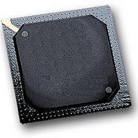
MPC564CZP40 Freescale Semiconductor, MPC564CZP40 Datasheet - Page 498

MPC564CZP40
Manufacturer Part Number
MPC564CZP40
Description
IC MPU 32BIT W/CODE COMP 388PBGA
Manufacturer
Freescale Semiconductor
Series
MPC5xxr
Specifications of MPC564CZP40
Core Processor
PowerPC
Core Size
32-Bit
Speed
40MHz
Connectivity
CAN, EBI/EMI, SCI, SPI, UART/USART
Peripherals
POR, PWM, WDT
Number Of I /o
56
Program Memory Size
512KB (512K x 8)
Program Memory Type
FLASH
Ram Size
32K x 8
Voltage - Supply (vcc/vdd)
2.5 V ~ 2.7 V
Data Converters
A/D 32x10b
Oscillator Type
External
Operating Temperature
-40°C ~ 85°C
Package / Case
388-BGA
Processor Series
MPC5xx
Core
PowerPC
Data Bus Width
32 bit
Data Ram Size
32 KB
Interface Type
CAN, JTAG, QSPI, SCI, SPI, UART
Maximum Clock Frequency
40 MHz
Number Of Programmable I/os
56
Number Of Timers
2
Operating Supply Voltage
0 V to 5 V
Maximum Operating Temperature
+ 85 C
Mounting Style
SMD/SMT
Minimum Operating Temperature
- 40 C
On-chip Adc
2 (10 bit, 32 Channel)
For Use With
MPC564EVB - KIT EVAL FOR MPC561/562/563/564
Lead Free Status / RoHS Status
Contains lead / RoHS non-compliant
Eeprom Size
-
Lead Free Status / Rohs Status
No
Available stocks
Company
Part Number
Manufacturer
Quantity
Price
Company:
Part Number:
MPC564CZP40
Manufacturer:
Freescale Semiconductor
Quantity:
10 000
- Current page: 498 of 1420
- Download datasheet (11Mb)
QADC64E Legacy Mode Operation
corresponding locations in the result word table as scratch pad RAM, remembering that only 10 bits are
implemented. The result alignment is only implemented for software read operations. Since write
operations are not the normal use for the result registers, only one write data format is supported, which is
right justified data.
13.4
This section describes the QADC64E analog subsystem, which includes the front-end analog multiplexer
and analog-to-digital converter.
13.4.1
The analog subsystem consists of the path from the input signals to the A/D converter block. Signals from
the queue control logic are fed to the multiplexer and state machine. The end of convert (EOC) signal and
the successive-approximation register (SAR) are the result of the conversion.
diagram of the QADC64E analog subsystem.
13-34
Analog Subsystem
Analog-to-Digital Converter Operation
Some write operations, like bit manipulation, may not operate as expected
because the hardware cannot access a true 16-bit value.
AN44
AN59
V
V
.
. .
RH
RL
Figure 13-20. QADC64E Analog Subsystem Block Diagram
CCW Buffer
Data Bus
CHAN
Decoder
6
10
MPC561/MPC563 Reference Manual, Rev. 1.2
Sample
REF
IST
+
-
Result
Buffer
AMP
State Mach, SAR and SAR Buffer
RDAC
(7 BIT)
NOTE
7
Standard Converter Interface
CONV.
Final
Buffer
WCCW EOS/EOC
STOP
Sample
CAP Array
Equals CDAC
CRH
CRL
CDAC
(4 BIT)
4 (one is offset)
CLK
BIAS
Figure 13-20
-
+
COMP.
Zero
Freescale Semiconductor
2
shows a block
Related parts for MPC564CZP40
Image
Part Number
Description
Manufacturer
Datasheet
Request
R

Part Number:
Description:
MPC5 1K0 5%
Manufacturer:
TE Connectivity
Datasheet:

Part Number:
Description:
MPC5 500R 5%
Manufacturer:
TE Connectivity
Datasheet:

Part Number:
Description:
MPC5 5K0 5%
Manufacturer:
Tyco Electronics
Datasheet:

Part Number:
Description:
MPC5 5R0 5%
Manufacturer:
Tyco Electronics
Datasheet:

Part Number:
Description:
MPC5 50K 5%
Manufacturer:
Tyco Electronics
Datasheet:

Part Number:
Description:
MPC5 1R0 5%
Manufacturer:
Tyco Electronics
Datasheet:
Part Number:
Description:
Manufacturer:
Freescale Semiconductor, Inc
Datasheet:
Part Number:
Description:
Manufacturer:
Freescale Semiconductor, Inc
Datasheet:
Part Number:
Description:
Manufacturer:
Freescale Semiconductor, Inc
Datasheet:
Part Number:
Description:
Manufacturer:
Freescale Semiconductor, Inc
Datasheet:
Part Number:
Description:
Manufacturer:
Freescale Semiconductor, Inc
Datasheet:


