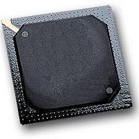
MPC564CZP40 Freescale Semiconductor, MPC564CZP40 Datasheet - Page 664

MPC564CZP40
Manufacturer Part Number
MPC564CZP40
Description
IC MPU 32BIT W/CODE COMP 388PBGA
Manufacturer
Freescale Semiconductor
Series
MPC5xxr
Specifications of MPC564CZP40
Core Processor
PowerPC
Core Size
32-Bit
Speed
40MHz
Connectivity
CAN, EBI/EMI, SCI, SPI, UART/USART
Peripherals
POR, PWM, WDT
Number Of I /o
56
Program Memory Size
512KB (512K x 8)
Program Memory Type
FLASH
Ram Size
32K x 8
Voltage - Supply (vcc/vdd)
2.5 V ~ 2.7 V
Data Converters
A/D 32x10b
Oscillator Type
External
Operating Temperature
-40°C ~ 85°C
Package / Case
388-BGA
Processor Series
MPC5xx
Core
PowerPC
Data Bus Width
32 bit
Data Ram Size
32 KB
Interface Type
CAN, JTAG, QSPI, SCI, SPI, UART
Maximum Clock Frequency
40 MHz
Number Of Programmable I/os
56
Number Of Timers
2
Operating Supply Voltage
0 V to 5 V
Maximum Operating Temperature
+ 85 C
Mounting Style
SMD/SMT
Minimum Operating Temperature
- 40 C
On-chip Adc
2 (10 bit, 32 Channel)
For Use With
MPC564EVB - KIT EVAL FOR MPC561/562/563/564
Lead Free Status / RoHS Status
Contains lead / RoHS non-compliant
Eeprom Size
-
Lead Free Status / Rohs Status
No
Available stocks
Company
Part Number
Manufacturer
Quantity
Price
Company:
Part Number:
MPC564CZP40
Manufacturer:
Freescale Semiconductor
Quantity:
10 000
- Current page: 664 of 1420
- Download datasheet (11Mb)
Queued Serial Multi-Channel Module
*Reads access the RDRx; writes access the TDRx.
During SCIx initialization, two bits in the SCCxR1 should be written last: the transmitter enable (TE) and
receiver enable (RE) bits, which enable SCIx. Registers SCCxR0 and SCCxR1 should both be initialized
at the same time or before TE and RE are asserted. A single half-word write to SCCxR1 can be used to
initialize SCIx and enable the transmitter and receiver.
15.7.2
SCCxR0 contains the SCIx baud rate selection field and two bits controlling the clock source. The baud
rate must be set before the SCI is enabled. The CPU can read and write SCCxR0 at any time.
Changing the value of SCCxR0 bits during a transfer operation can disrupt the transfer. Before changing
register values, allow the SCI to complete the current transfer, then disable the receiver and transmitter.
15-46
SRESET
Bits
3:15
0
1
2
Field OTHR
Addr
SCI Control Register 0 (SCCxR0)
LNKBD
SCxBR
MSB
OTHR
Name
0
0
—
0x30 504C-6A
0x30 502C —
0x30 504A
LNKBD
This bit is reserved and should always be programmed to 0.
This bit is reserved and should always be programmed to 0.
Reserved
SCI baud rate. The SCI baud rate is programmed by writing a 13-bit value to this field. Writing a
value of zero to SCxBR disables the baud rate generator. Baud clock rate is calculated as follows:
where SCxBR is in the range of 1 to 8191.
Refer to Section 15.7.7.3, “Baud Clock,” for more information.
0
1
Figure 15-26. SCCxR0 — SCI Control Register 0
—
0
2
MPC561/MPC563 Reference Manual, Rev. 1.2
Table 15-24. SCCxR0 Bit Descriptions
QSCI1 Transmit Queue
QSCI1 Receive Queue
3
Table 15-23. SCI Registers
Memory Area
Memory Area
4
5
0x30 5008; 0x30 5020
SCI Baud Rate
6
QSCI1 Transmit Queue Data locations (on
half-word boundary)
QSCI1 Receive Queue Data locations (on
half-word boundary)
Description
7
0_0000_0000_0100
8
=
----------------------------- -
32xSCxBR
SCxBR
f SYS
9
10
11
12
Freescale Semiconductor
13
14
LSB
15
Related parts for MPC564CZP40
Image
Part Number
Description
Manufacturer
Datasheet
Request
R

Part Number:
Description:
MPC5 1K0 5%
Manufacturer:
TE Connectivity
Datasheet:

Part Number:
Description:
MPC5 500R 5%
Manufacturer:
TE Connectivity
Datasheet:

Part Number:
Description:
MPC5 5K0 5%
Manufacturer:
Tyco Electronics
Datasheet:

Part Number:
Description:
MPC5 5R0 5%
Manufacturer:
Tyco Electronics
Datasheet:

Part Number:
Description:
MPC5 50K 5%
Manufacturer:
Tyco Electronics
Datasheet:

Part Number:
Description:
MPC5 1R0 5%
Manufacturer:
Tyco Electronics
Datasheet:
Part Number:
Description:
Manufacturer:
Freescale Semiconductor, Inc
Datasheet:
Part Number:
Description:
Manufacturer:
Freescale Semiconductor, Inc
Datasheet:
Part Number:
Description:
Manufacturer:
Freescale Semiconductor, Inc
Datasheet:
Part Number:
Description:
Manufacturer:
Freescale Semiconductor, Inc
Datasheet:
Part Number:
Description:
Manufacturer:
Freescale Semiconductor, Inc
Datasheet:


