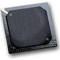
MPC564CZP40 Freescale Semiconductor, MPC564CZP40 Datasheet - Page 528

MPC564CZP40
Manufacturer Part Number
MPC564CZP40
Description
IC MPU 32BIT W/CODE COMP 388PBGA
Manufacturer
Freescale Semiconductor
Series
MPC5xxr
Specifications of MPC564CZP40
Core Processor
PowerPC
Core Size
32-Bit
Speed
40MHz
Connectivity
CAN, EBI/EMI, SCI, SPI, UART/USART
Peripherals
POR, PWM, WDT
Number Of I /o
56
Program Memory Size
512KB (512K x 8)
Program Memory Type
FLASH
Ram Size
32K x 8
Voltage - Supply (vcc/vdd)
2.5 V ~ 2.7 V
Data Converters
A/D 32x10b
Oscillator Type
External
Operating Temperature
-40°C ~ 85°C
Package / Case
388-BGA
Processor Series
MPC5xx
Core
PowerPC
Data Bus Width
32 bit
Data Ram Size
32 KB
Interface Type
CAN, JTAG, QSPI, SCI, SPI, UART
Maximum Clock Frequency
40 MHz
Number Of Programmable I/os
56
Number Of Timers
2
Operating Supply Voltage
0 V to 5 V
Maximum Operating Temperature
+ 85 C
Mounting Style
SMD/SMT
Minimum Operating Temperature
- 40 C
On-chip Adc
2 (10 bit, 32 Channel)
For Use With
MPC564EVB - KIT EVAL FOR MPC561/562/563/564
Lead Free Status / RoHS Status
Contains lead / RoHS non-compliant
Eeprom Size
-
Lead Free Status / Rohs Status
No
Available stocks
Company
Part Number
Manufacturer
Quantity
Price
Company:
Part Number:
MPC564CZP40
Manufacturer:
Freescale Semiconductor
Quantity:
10 000
- Current page: 528 of 1420
- Download datasheet (11Mb)
QADC64E Legacy Mode Operation
Recall QS = 0 => Queues disabled; QS = 8 => Q1 active, Q2 disabled; QS= 4 => Q1 paused, Q2 disabled.
A time separator was provided between the triggers and end of conversion (EOC). The relationship to
QCLK displayed is not guaranteed.
CWPQ1 and CWPQ2 typically lag CWP and only match CWP when the associated queue is inactive.
Another way to view CWPQ1 and CWPQ2 is that these registers update when EOC triggers the result
register to be written.
When the pause bit is set (CCW0), please note that CWP does not increment until triggered. When the
pause is not set (CCW1), the CWP increments with EOC.
The conversion results Q1 RES(x) show the result associated with CCW(x). So that R0 represents the
result associated with CCW0.
Example 2 below shows the timing for conversions in gated mode single-scan with the
same assumptions as example 1 except:
When the gate closes and opens again the conversions start with the first CCW in Q1.
When the gate closes the active conversion completes before the queue goes idle.
When Q1 completes both the CF1 bit sets and the SSE bit clears.
13-64
•
•
•
•
QCLK
Trig1
EOC
QS
CWP
CWPQ1
Q1 RES
Q1 RES shows relative result register updates
No pause bits set in any CCW
External trigger gated single-scan mode for Q1
Single-scan bit is set
LAST
0
Figure 13-46. External Trigger Mode (Positive Edge) Timing with Pause
LAST
4
8
MPC561/MPC563 Reference Manual, Rev. 1.2
CCW0
Conversion time is >= 14 QCLKS
Time between triggers
4
R0
CCW0
CCW1
8
Freescale Semiconductor
CCW1
R1
CCW2
Related parts for MPC564CZP40
Image
Part Number
Description
Manufacturer
Datasheet
Request
R

Part Number:
Description:
MPC5 1K0 5%
Manufacturer:
TE Connectivity
Datasheet:

Part Number:
Description:
MPC5 500R 5%
Manufacturer:
TE Connectivity
Datasheet:

Part Number:
Description:
MPC5 5K0 5%
Manufacturer:
Tyco Electronics
Datasheet:

Part Number:
Description:
MPC5 5R0 5%
Manufacturer:
Tyco Electronics
Datasheet:

Part Number:
Description:
MPC5 50K 5%
Manufacturer:
Tyco Electronics
Datasheet:

Part Number:
Description:
MPC5 1R0 5%
Manufacturer:
Tyco Electronics
Datasheet:
Part Number:
Description:
Manufacturer:
Freescale Semiconductor, Inc
Datasheet:
Part Number:
Description:
Manufacturer:
Freescale Semiconductor, Inc
Datasheet:
Part Number:
Description:
Manufacturer:
Freescale Semiconductor, Inc
Datasheet:
Part Number:
Description:
Manufacturer:
Freescale Semiconductor, Inc
Datasheet:
Part Number:
Description:
Manufacturer:
Freescale Semiconductor, Inc
Datasheet:


