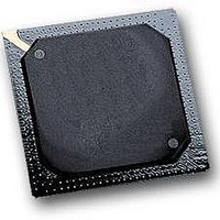
MPC564CZP40 Freescale Semiconductor, MPC564CZP40 Datasheet - Page 857

MPC564CZP40
Manufacturer Part Number
MPC564CZP40
Description
IC MPU 32BIT W/CODE COMP 388PBGA
Manufacturer
Freescale Semiconductor
Series
MPC5xxr
Specifications of MPC564CZP40
Core Processor
PowerPC
Core Size
32-Bit
Speed
40MHz
Connectivity
CAN, EBI/EMI, SCI, SPI, UART/USART
Peripherals
POR, PWM, WDT
Number Of I /o
56
Program Memory Size
512KB (512K x 8)
Program Memory Type
FLASH
Ram Size
32K x 8
Voltage - Supply (vcc/vdd)
2.5 V ~ 2.7 V
Data Converters
A/D 32x10b
Oscillator Type
External
Operating Temperature
-40°C ~ 85°C
Package / Case
388-BGA
Processor Series
MPC5xx
Core
PowerPC
Data Bus Width
32 bit
Data Ram Size
32 KB
Interface Type
CAN, JTAG, QSPI, SCI, SPI, UART
Maximum Clock Frequency
40 MHz
Number Of Programmable I/os
56
Number Of Timers
2
Operating Supply Voltage
0 V to 5 V
Maximum Operating Temperature
+ 85 C
Mounting Style
SMD/SMT
Minimum Operating Temperature
- 40 C
On-chip Adc
2 (10 bit, 32 Channel)
For Use With
MPC564EVB - KIT EVAL FOR MPC561/562/563/564
Lead Free Status / RoHS Status
Contains lead / RoHS non-compliant
Eeprom Size
-
Lead Free Status / Rohs Status
No
Available stocks
Company
Part Number
Manufacturer
Quantity
Price
Company:
Part Number:
MPC564CZP40
Manufacturer:
Freescale Semiconductor
Quantity:
10 000
- Current page: 857 of 1420
- Download datasheet (11Mb)
The DPTRAM array occupies an 8-Kbyte block. In the MPC561/MPC563, the array must be located at the
address 0x30 2000. Refer to
20.3.1
This register defines the basic configuration of the DPTRAM module. The DPTMCR contains bits to
configure the DPTRAM module for stop operation and for proper access privileges to the array. The
register also contains the MISC control bits.
Freescale Semiconductor
SRESET
Supervisor R/W
Test
Supervisor R/W
Supervisor
Read Only
Supervisor
Read Only
Supervisor
Read Only
Field STOP
Addr
R/W Access
DPTRAM Module Configuration Register (DPTMCR)
MSB
0
0
1
Figure 20-3. DPT Module Configuration Register (DPTMCR)
0x30 000A
0x30 0000
0x30 0002
0x30 0004
0x30 0006
0x30 0008
Undefined
Address
2
—
Figure 1-3
3
MPC561/MPC563 Reference Manual, Rev. 1.2
Figure 20-2. DPTRAM Memory Map
Table 20-1. DPTRAM Register Map
0x30 2000
0x30 3FFF
DPT RAM Module Configuration Register (DPTRMCR)
See
Test Configuration Register (DPTTCR)
RAM Base Address Register (RAMBAR)
See
Multiple Input Signature Register High (MISRH)
See
Registers
Multiple Input Signature Register Low (MISRL)
See
Registers
Multiple Input Signature Counter (MISCNT)
See
descriptions.
4
and
Table 20-2
Table 20-3
Section 20.3.4, “MISR High (MISRH) and MISR Low
Section 20.3.4, “MISR High (MISRH) and MISR Low
Section 20.3.5, “MISC Counter
MISF MISEN RASP
0
5
Figure
(MISRL)” for bit descriptions.
(MISRL)” for bit descriptions.
DPTRAM Array
0
6
for bit descriptions.
for bit descriptions.
20-2.
(8 Kbytes)
0x30 0000
1
7
Register
8
(MISCNT)” for bit
9
10
0000_0000
11
Dual-Port TPU3 RAM (DPTRAM)
—
12
Last memory
Reset Value
13
address
0x0100
0x0000
0x0001
0x0000
0x0000
14
LSB
15
20-3
Related parts for MPC564CZP40
Image
Part Number
Description
Manufacturer
Datasheet
Request
R

Part Number:
Description:
MPC5 1K0 5%
Manufacturer:
TE Connectivity
Datasheet:

Part Number:
Description:
MPC5 500R 5%
Manufacturer:
TE Connectivity
Datasheet:

Part Number:
Description:
MPC5 5K0 5%
Manufacturer:
Tyco Electronics
Datasheet:

Part Number:
Description:
MPC5 5R0 5%
Manufacturer:
Tyco Electronics
Datasheet:

Part Number:
Description:
MPC5 50K 5%
Manufacturer:
Tyco Electronics
Datasheet:

Part Number:
Description:
MPC5 1R0 5%
Manufacturer:
Tyco Electronics
Datasheet:
Part Number:
Description:
Manufacturer:
Freescale Semiconductor, Inc
Datasheet:
Part Number:
Description:
Manufacturer:
Freescale Semiconductor, Inc
Datasheet:
Part Number:
Description:
Manufacturer:
Freescale Semiconductor, Inc
Datasheet:
Part Number:
Description:
Manufacturer:
Freescale Semiconductor, Inc
Datasheet:
Part Number:
Description:
Manufacturer:
Freescale Semiconductor, Inc
Datasheet:


