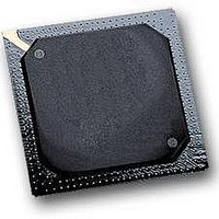
MPC564CZP40 Freescale Semiconductor, MPC564CZP40 Datasheet - Page 112

MPC564CZP40
Manufacturer Part Number
MPC564CZP40
Description
IC MPU 32BIT W/CODE COMP 388PBGA
Manufacturer
Freescale Semiconductor
Series
MPC5xxr
Specifications of MPC564CZP40
Core Processor
PowerPC
Core Size
32-Bit
Speed
40MHz
Connectivity
CAN, EBI/EMI, SCI, SPI, UART/USART
Peripherals
POR, PWM, WDT
Number Of I /o
56
Program Memory Size
512KB (512K x 8)
Program Memory Type
FLASH
Ram Size
32K x 8
Voltage - Supply (vcc/vdd)
2.5 V ~ 2.7 V
Data Converters
A/D 32x10b
Oscillator Type
External
Operating Temperature
-40°C ~ 85°C
Package / Case
388-BGA
Processor Series
MPC5xx
Core
PowerPC
Data Bus Width
32 bit
Data Ram Size
32 KB
Interface Type
CAN, JTAG, QSPI, SCI, SPI, UART
Maximum Clock Frequency
40 MHz
Number Of Programmable I/os
56
Number Of Timers
2
Operating Supply Voltage
0 V to 5 V
Maximum Operating Temperature
+ 85 C
Mounting Style
SMD/SMT
Minimum Operating Temperature
- 40 C
On-chip Adc
2 (10 bit, 32 Channel)
For Use With
MPC564EVB - KIT EVAL FOR MPC561/562/563/564
Lead Free Status / RoHS Status
Contains lead / RoHS non-compliant
Eeprom Size
-
Lead Free Status / Rohs Status
No
Available stocks
Company
Part Number
Manufacturer
Quantity
Price
Company:
Part Number:
MPC564CZP40
Manufacturer:
Freescale Semiconductor
Quantity:
10 000
- Current page: 112 of 1420
- Download datasheet (11Mb)
Signal Descriptions
2-14
ALTREF
VDDA
VSSA
PCS0 / SS / QGPIO0
PCS[1:3] / QGPIO[1:3]
MISO / QGPIO4
MOSI / QGPIO5
SCK / QGPIO6
TXD1 / QGPO1
Signal Name
Table 2-1. MPC561/MPC563 Signal Descriptions (continued)
Signals
No. of
1
1
1
1
3
1
1
1
1
MPC561/MPC563 Reference Manual, Rev. 1.2
Type
I/O
I/O
I/O
I/O
I/O
I/O
I/O
I/O
I/O
I/O
I/O
O
O
I
I
I
ALTREF
VDDA
VSSA
QGPIO0
QGPIO[1:3]
QGPIO4
QGPIO5
QGPIO6
QGPO1
Function after
Reset
QSMCM
1
ALTREF. Input signal for alternate reference voltage for the
QADC64E_A and QADC64E_B modules.
VDDA. Power supply input to analog subsystems of the
QADC64E_A and QADC64E_B modules.
VSSA. Ground level for analog subsystems of the
QADC64E_A and QADC64E_B modules.
PCS0. This signal provides QSPI peripheral chip select 0 for
the QSMCM module.
SS. Assertion of this bidirectional signal places the QSPI in
slave mode.
Port QGPIO0. When this signal is not needed for a QSPI
application it can be configured as a general-purpose
input/output.
PCS[1:3]. These signals provide QSPI peripheral chip
selects for the QSMCM module.
Port QGPIO[1:3]. When these signals are not needed for
QSPI applications they can be configured as
general-purpose input/outputs.
Master-In Slave-Out (MISO). This bidirectional signal is the
serial data input to the QSPI in master mode, and serial data
output from the QSPI in slave mode.
Port QGPIO4. When this signal is not needed for a QSPI
application it can be configured as a general-purpose
input/output.
Master-Out Slave-In (MOSI). This bidirectional signal is the
serial data output from the QSPI in master mode and serial
data input to the QSPI in slave mode.
Port QGPIO5. When this signal is not needed for a QSPI
application it can be configured as a general-purpose
input/output.
SCK. This bidirectional signal is the clock from the QSPI in
master mode or is the clock to the QSPI in slave mode.
Port QGPIO6 for the QSMCM module. When this signal is
not needed for a QSPI application it can be configured as a
general-purpose input/output. When the QSPI is enabled for
serial transmitting, the signal cannot function as a GPIO.
Transmit Data 1. This is the serial data output from the SCI1.
Port QGPO 1. When these signals are not needed for SCI
applications, they can be configured as general-purpose
outputs. When the transmit enable bit in the SCI control
register is set to a logic 1, these signals cannot function as
general-purpose outputs.
Description
Freescale Semiconductor
Related parts for MPC564CZP40
Image
Part Number
Description
Manufacturer
Datasheet
Request
R

Part Number:
Description:
MPC5 1K0 5%
Manufacturer:
TE Connectivity
Datasheet:

Part Number:
Description:
MPC5 500R 5%
Manufacturer:
TE Connectivity
Datasheet:

Part Number:
Description:
MPC5 5K0 5%
Manufacturer:
Tyco Electronics
Datasheet:

Part Number:
Description:
MPC5 5R0 5%
Manufacturer:
Tyco Electronics
Datasheet:

Part Number:
Description:
MPC5 50K 5%
Manufacturer:
Tyco Electronics
Datasheet:

Part Number:
Description:
MPC5 1R0 5%
Manufacturer:
Tyco Electronics
Datasheet:
Part Number:
Description:
Manufacturer:
Freescale Semiconductor, Inc
Datasheet:
Part Number:
Description:
Manufacturer:
Freescale Semiconductor, Inc
Datasheet:
Part Number:
Description:
Manufacturer:
Freescale Semiconductor, Inc
Datasheet:
Part Number:
Description:
Manufacturer:
Freescale Semiconductor, Inc
Datasheet:
Part Number:
Description:
Manufacturer:
Freescale Semiconductor, Inc
Datasheet:


