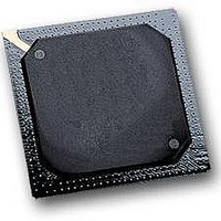
MPC564CZP40 Freescale Semiconductor, MPC564CZP40 Datasheet - Page 220

MPC564CZP40
Manufacturer Part Number
MPC564CZP40
Description
IC MPU 32BIT W/CODE COMP 388PBGA
Manufacturer
Freescale Semiconductor
Series
MPC5xxr
Specifications of MPC564CZP40
Core Processor
PowerPC
Core Size
32-Bit
Speed
40MHz
Connectivity
CAN, EBI/EMI, SCI, SPI, UART/USART
Peripherals
POR, PWM, WDT
Number Of I /o
56
Program Memory Size
512KB (512K x 8)
Program Memory Type
FLASH
Ram Size
32K x 8
Voltage - Supply (vcc/vdd)
2.5 V ~ 2.7 V
Data Converters
A/D 32x10b
Oscillator Type
External
Operating Temperature
-40°C ~ 85°C
Package / Case
388-BGA
Processor Series
MPC5xx
Core
PowerPC
Data Bus Width
32 bit
Data Ram Size
32 KB
Interface Type
CAN, JTAG, QSPI, SCI, SPI, UART
Maximum Clock Frequency
40 MHz
Number Of Programmable I/os
56
Number Of Timers
2
Operating Supply Voltage
0 V to 5 V
Maximum Operating Temperature
+ 85 C
Mounting Style
SMD/SMT
Minimum Operating Temperature
- 40 C
On-chip Adc
2 (10 bit, 32 Channel)
For Use With
MPC564EVB - KIT EVAL FOR MPC561/562/563/564
Lead Free Status / RoHS Status
Contains lead / RoHS non-compliant
Eeprom Size
-
Lead Free Status / Rohs Status
No
Available stocks
Company
Part Number
Manufacturer
Quantity
Price
Company:
Part Number:
MPC564CZP40
Manufacturer:
Freescale Semiconductor
Quantity:
10 000
- Current page: 220 of 1420
- Download datasheet (11Mb)
Burst Buffer Controller 2 Module
U-bus access mode of the RAM is activated by the BBCMCR[DCAE] bit setting (see
“BBC Module Configuration Register
the U-bus and cannot be accessed by the ICDU logic.
In this mode:
4.4.1.1
The DECRAM module does not acknowledge U-bus accesses that violate the configuration defined in the
BBCMCR. This causes the machine check exception for the internal RCPU or an error condition for the
MPC561/MPC563 external master.
4.4.1.2
The bus interface and DECRAM control logic are powered by V
by a separate power pin (IRAMSTBY).
4.5
The burst buffer controller contains a branch target buffer (BTB) to reduce the impact of branches on
processor performance. Following is a summary of the BTB features:
The BTB consists of eight branch target entries (BTE). Refer to
fully associative cache. Each entry contains a tag and several data buffers related to this tag.
4.5.1
When the RCPU generates a change of flow (COF) address for instruction fetch, the BTB control logic
compares it to the tag values currently stored in the tag register file where the following events can happen:
4-14
•
•
•
•
•
•
•
The DECRAM supports word, half-word and byte operations.
The DECRAM is emulated to be 32 bits wide. For example: a load access from offset 0 in the
DECRAM will deliver the concatenation of the first word in each of the DECRAM banks when
RAM 1 contains the 16 LSB of the word and RAM 2 contains the 16 MSB.
Load accesses at any width are supplied with 32 bits of valid data.
The DECRAM communicates with the U-bus pipeline but does not support pipelined accesses to
itself. If a store operation is second in the U-bus pipe, the store is carried out immediately and the
U-bus acknowledgment is performed when the previous transaction in the pipe completes.
Burst access is not supported.
Software controlled BTB enable/disable, inhibit, and invalidate
User transparent — no user management required
Branch Target Buffer
BTB Operation
Memory Protection Violations
DECRAM Standby Operation Mode
Instructions running from the DECRAM should not also perform store
operations to the DECRAM.
MPC561/MPC563 Reference Manual, Rev. 1.2
(BBCMCR)”). In this mode the DECRAM can be accessed from
NOTE
DD
Figure
supply. The memory array is supplied
4-5. All entries are managed as a
Freescale Semiconductor
Section 4.6.2.1,
Related parts for MPC564CZP40
Image
Part Number
Description
Manufacturer
Datasheet
Request
R

Part Number:
Description:
MPC5 1K0 5%
Manufacturer:
TE Connectivity
Datasheet:

Part Number:
Description:
MPC5 500R 5%
Manufacturer:
TE Connectivity
Datasheet:

Part Number:
Description:
MPC5 5K0 5%
Manufacturer:
Tyco Electronics
Datasheet:

Part Number:
Description:
MPC5 5R0 5%
Manufacturer:
Tyco Electronics
Datasheet:

Part Number:
Description:
MPC5 50K 5%
Manufacturer:
Tyco Electronics
Datasheet:

Part Number:
Description:
MPC5 1R0 5%
Manufacturer:
Tyco Electronics
Datasheet:
Part Number:
Description:
Manufacturer:
Freescale Semiconductor, Inc
Datasheet:
Part Number:
Description:
Manufacturer:
Freescale Semiconductor, Inc
Datasheet:
Part Number:
Description:
Manufacturer:
Freescale Semiconductor, Inc
Datasheet:
Part Number:
Description:
Manufacturer:
Freescale Semiconductor, Inc
Datasheet:
Part Number:
Description:
Manufacturer:
Freescale Semiconductor, Inc
Datasheet:


