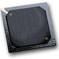
MPC564CZP40 Freescale Semiconductor, MPC564CZP40 Datasheet - Page 1227

MPC564CZP40
Manufacturer Part Number
MPC564CZP40
Description
IC MPU 32BIT W/CODE COMP 388PBGA
Manufacturer
Freescale Semiconductor
Series
MPC5xxr
Specifications of MPC564CZP40
Core Processor
PowerPC
Core Size
32-Bit
Speed
40MHz
Connectivity
CAN, EBI/EMI, SCI, SPI, UART/USART
Peripherals
POR, PWM, WDT
Number Of I /o
56
Program Memory Size
512KB (512K x 8)
Program Memory Type
FLASH
Ram Size
32K x 8
Voltage - Supply (vcc/vdd)
2.5 V ~ 2.7 V
Data Converters
A/D 32x10b
Oscillator Type
External
Operating Temperature
-40°C ~ 85°C
Package / Case
388-BGA
Processor Series
MPC5xx
Core
PowerPC
Data Bus Width
32 bit
Data Ram Size
32 KB
Interface Type
CAN, JTAG, QSPI, SCI, SPI, UART
Maximum Clock Frequency
40 MHz
Number Of Programmable I/os
56
Number Of Timers
2
Operating Supply Voltage
0 V to 5 V
Maximum Operating Temperature
+ 85 C
Mounting Style
SMD/SMT
Minimum Operating Temperature
- 40 C
On-chip Adc
2 (10 bit, 32 Channel)
For Use With
MPC564EVB - KIT EVAL FOR MPC561/562/563/564
Lead Free Status / RoHS Status
Contains lead / RoHS non-compliant
Eeprom Size
-
Lead Free Status / Rohs Status
No
Available stocks
Company
Part Number
Manufacturer
Quantity
Price
Company:
Part Number:
MPC564CZP40
Manufacturer:
Freescale Semiconductor
Quantity:
10 000
- Current page: 1227 of 1420
- Download datasheet (11Mb)
F.6
Note: (V
Freescale Semiconductor
18
19
20
21
22
23
24
25
26
27
1
2
3
1
2
3
4
5
6
7
8
9
This parameter is periodically sampled rather than 100% tested
Up to 0.5 V during power up/down.
To obtain full-range results, V
When using the QADC in legacy mode it is recommended to connect this pin to 2.6V or 3.3V, however it can be
connected to 0V or 5V without damage to the device.
A resistor must be placed in series with the IRAMSTBY power supply. Refer to
Guidelines.”
All injection current is transferred to the V
power supply within the specified voltage range.
Absolute maximum voltage ratings for each pin (see
Total injection current for all I/O pins on the chip must not exceed 20 mA (sustained current). Exceeding this limit can
cause disruption of normal operation.
Current refers to two QADC64 modules operating simultaneously.
Below disruptive current conditions, the channel being stressed has conversion values of 0x3FF for analog inputs
greater than V
presence of the sample amplifier. Other channels are not affected by non-disruptive conditions.
Assumes stable power and oscillator.
F
Estimated value, real values to be characterized and updated.
VCOOUT
DD
Oscillator Startup time (for typical crystal capacitive load)
4-MHz crystal
20-MHz crystal
PLL Lock Time
PLL Operating Range
Crystal Operating Range, MODCK=0b010,0b110
MODCK[1:3] = 0b001, 0b011, 0b100, 0b101, 0b111
PLL Jitter
PLL Jitter (averaged over 10 µs)
Limp Mode Clock Out Frequency
Oscillator Bias Current (XTAL)
4 MHz
20 MHz
Oscillator Drive (XTAL)
Oscillator Bias Resistor
Oscillator and PLL Electrical Characteristics
= 2.6 V ± 0.1 V, V
is 2x the system frequency.
RH
and 0x000 for values less than V
DDH
Characteristic
2
= 5.0 V ± 0.25 V, T
SSA
MPC561/MPC563 Reference Manual, Rev. 1.2
≤ V
RL
≤ V
Table F-5. Oscillator and PLL
DDH
INDC
. An external load is required to dissipate this current to maintain the
A
= T
≤ V
RL
L
RH
Table
. This assumes that V
to T
≤ V
H
)
DDA
F-1) must also be met during this condition.
OSCstart20
OSCstart4
F
F
Symbol
CRYSTAL
VCOOUT
T
F
R
I
I
F
LOCK
BIAS
JIT10
OSC
—
OSC
JIT
RH
-0.3%
| 1.5 |
≤ V
Min
-1%
0.5
30
15
Appendix C, “Clock and Board
3
—
3
7
3
DDA
and V
Typica
11
1
l
RL
≥ V
Electrical Characteristics
SSA
+0.3%
1000
| 0.8 |
| 4.0 |
+1%
Max
112
17
10
10
25
—
5
3
due to the
3
1
Clocks
Input
MHz
MHz
MHz
MHz
Unit
MΩ
mA
mA
mA
ms
ms
—
F-11
Related parts for MPC564CZP40
Image
Part Number
Description
Manufacturer
Datasheet
Request
R

Part Number:
Description:
MPC5 1K0 5%
Manufacturer:
TE Connectivity
Datasheet:

Part Number:
Description:
MPC5 500R 5%
Manufacturer:
TE Connectivity
Datasheet:

Part Number:
Description:
MPC5 5K0 5%
Manufacturer:
Tyco Electronics
Datasheet:

Part Number:
Description:
MPC5 5R0 5%
Manufacturer:
Tyco Electronics
Datasheet:

Part Number:
Description:
MPC5 50K 5%
Manufacturer:
Tyco Electronics
Datasheet:

Part Number:
Description:
MPC5 1R0 5%
Manufacturer:
Tyco Electronics
Datasheet:
Part Number:
Description:
Manufacturer:
Freescale Semiconductor, Inc
Datasheet:
Part Number:
Description:
Manufacturer:
Freescale Semiconductor, Inc
Datasheet:
Part Number:
Description:
Manufacturer:
Freescale Semiconductor, Inc
Datasheet:
Part Number:
Description:
Manufacturer:
Freescale Semiconductor, Inc
Datasheet:
Part Number:
Description:
Manufacturer:
Freescale Semiconductor, Inc
Datasheet:


