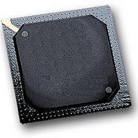
MPC564CZP40 Freescale Semiconductor, MPC564CZP40 Datasheet - Page 434

MPC564CZP40
Manufacturer Part Number
MPC564CZP40
Description
IC MPU 32BIT W/CODE COMP 388PBGA
Manufacturer
Freescale Semiconductor
Series
MPC5xxr
Specifications of MPC564CZP40
Core Processor
PowerPC
Core Size
32-Bit
Speed
40MHz
Connectivity
CAN, EBI/EMI, SCI, SPI, UART/USART
Peripherals
POR, PWM, WDT
Number Of I /o
56
Program Memory Size
512KB (512K x 8)
Program Memory Type
FLASH
Ram Size
32K x 8
Voltage - Supply (vcc/vdd)
2.5 V ~ 2.7 V
Data Converters
A/D 32x10b
Oscillator Type
External
Operating Temperature
-40°C ~ 85°C
Package / Case
388-BGA
Processor Series
MPC5xx
Core
PowerPC
Data Bus Width
32 bit
Data Ram Size
32 KB
Interface Type
CAN, JTAG, QSPI, SCI, SPI, UART
Maximum Clock Frequency
40 MHz
Number Of Programmable I/os
56
Number Of Timers
2
Operating Supply Voltage
0 V to 5 V
Maximum Operating Temperature
+ 85 C
Mounting Style
SMD/SMT
Minimum Operating Temperature
- 40 C
On-chip Adc
2 (10 bit, 32 Channel)
For Use With
MPC564EVB - KIT EVAL FOR MPC561/562/563/564
Lead Free Status / RoHS Status
Contains lead / RoHS non-compliant
Eeprom Size
-
Lead Free Status / Rohs Status
No
Available stocks
Company
Part Number
Manufacturer
Quantity
Price
Company:
Part Number:
MPC564CZP40
Manufacturer:
Freescale Semiconductor
Quantity:
10 000
- Current page: 434 of 1420
- Download datasheet (11Mb)
Memory Controller
10.9.5
10-36
,
1
HRESET
HRESET
The reset value is a reset configuration word value extracted from the indicated internal data bus lines. Refer to
28:30
Bits
Section 7.5.2, “Hard Reset Configuration Word
Bits
31
1:6
0
Field
Field
Addr
Dual-Mapping Base Register (DMBR)
MSB
—
16
0
Name
BSCY
0
TRLX
Name
BA
—
17
1
Burst beats length in clocks. This field determines the number of wait states inserted in all burst
beats except the first, when the GPCM starts handling the external memory access and thus
using SCY[0:3] as the main parameter for determining the length of that cycle.
The total cycle length may vary depending on the settings of other timing attributes.
The total memory access length for the beat is (1 + BSCY) x Clocks.
If an external TA response has been selected for this memory bank (by setting the SETA bit) then
BSCY[0:3] are not used.
000 0-clock-cycle (1 clock per data beat)
001 1-clock-cycle wait states (2 clocks per data beat)
010 2-clock-cycle wait states (3 clocks per data beat)
011 3-clock-cycle wait states (4 clocks per data beat)
1xx Reserved
Following a system reset, the BSCY bits are set to 0b011 in OR0.
Timing relaxed. This bit, when set, modifies the timing of the signals that control the memory
devices during a memory access to this memory region. Relaxed timing multiplies by two the
number of wait states determined by the SCY and BSCY fields. Refer to
“Summary of GPCM Timing
0 Normal timing is generated by the GPCM.
1 Relaxed timing is generated by the GPCM
Following a system reset, the TRLX bit is set in OR0.
Reserved
Base address. BA field corresponds to address bits [11:16]. The base address field is
compared (along with the address type field) to the address of the address bus to determine
whether an address should be dual-mapped by one of the memory banks controlled by the
memory controller. These bits are used in conjunction with the AM[11:16] bits in the DMOR.
18
2
Table 10-10. OR0–OR3 Bit Descriptions (continued)
Figure 10-25. Dual-Mapping Base Register (DMBR)
Undefined
19
3
BA
MPC561/MPC563 Reference Manual, Rev. 1.2
Table 10-11. DMBR Bit Descriptions
20
4
0000_0000_0000_0
21
5
—
(RCW).”
Options,” for a full list of the effects of this bit on signals timing.
22
6
0x2F C140
23
7
Description
000
Description
—
24
8
25
9
10
26
001
AT
11
27
12
28
Section 10.3.5,
DMCS
Freescale Semiconductor
13
29
ID20
1
14
000
30
—
ID31
DME
LSB
15
31
1
Related parts for MPC564CZP40
Image
Part Number
Description
Manufacturer
Datasheet
Request
R

Part Number:
Description:
MPC5 1K0 5%
Manufacturer:
TE Connectivity
Datasheet:

Part Number:
Description:
MPC5 500R 5%
Manufacturer:
TE Connectivity
Datasheet:

Part Number:
Description:
MPC5 5K0 5%
Manufacturer:
Tyco Electronics
Datasheet:

Part Number:
Description:
MPC5 5R0 5%
Manufacturer:
Tyco Electronics
Datasheet:

Part Number:
Description:
MPC5 50K 5%
Manufacturer:
Tyco Electronics
Datasheet:

Part Number:
Description:
MPC5 1R0 5%
Manufacturer:
Tyco Electronics
Datasheet:
Part Number:
Description:
Manufacturer:
Freescale Semiconductor, Inc
Datasheet:
Part Number:
Description:
Manufacturer:
Freescale Semiconductor, Inc
Datasheet:
Part Number:
Description:
Manufacturer:
Freescale Semiconductor, Inc
Datasheet:
Part Number:
Description:
Manufacturer:
Freescale Semiconductor, Inc
Datasheet:
Part Number:
Description:
Manufacturer:
Freescale Semiconductor, Inc
Datasheet:


