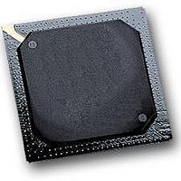
MPC564CZP40 Freescale Semiconductor, MPC564CZP40 Datasheet - Page 663

MPC564CZP40
Manufacturer Part Number
MPC564CZP40
Description
IC MPU 32BIT W/CODE COMP 388PBGA
Manufacturer
Freescale Semiconductor
Series
MPC5xxr
Specifications of MPC564CZP40
Core Processor
PowerPC
Core Size
32-Bit
Speed
40MHz
Connectivity
CAN, EBI/EMI, SCI, SPI, UART/USART
Peripherals
POR, PWM, WDT
Number Of I /o
56
Program Memory Size
512KB (512K x 8)
Program Memory Type
FLASH
Ram Size
32K x 8
Voltage - Supply (vcc/vdd)
2.5 V ~ 2.7 V
Data Converters
A/D 32x10b
Oscillator Type
External
Operating Temperature
-40°C ~ 85°C
Package / Case
388-BGA
Processor Series
MPC5xx
Core
PowerPC
Data Bus Width
32 bit
Data Ram Size
32 KB
Interface Type
CAN, JTAG, QSPI, SCI, SPI, UART
Maximum Clock Frequency
40 MHz
Number Of Programmable I/os
56
Number Of Timers
2
Operating Supply Voltage
0 V to 5 V
Maximum Operating Temperature
+ 85 C
Mounting Style
SMD/SMT
Minimum Operating Temperature
- 40 C
On-chip Adc
2 (10 bit, 32 Channel)
For Use With
MPC564EVB - KIT EVAL FOR MPC561/562/563/564
Lead Free Status / RoHS Status
Contains lead / RoHS non-compliant
Eeprom Size
-
Lead Free Status / Rohs Status
No
Available stocks
Company
Part Number
Manufacturer
Quantity
Price
Company:
Part Number:
MPC564CZP40
Manufacturer:
Freescale Semiconductor
Quantity:
10 000
- Current page: 663 of 1420
- Download datasheet (11Mb)
15.7.1
The SCI programming model includes the QSMCM global and pin control registers and the DSCI
registers.
The DSCI registers, listed in
data registers. All registers may be read or written at any time by the CPU. Rewriting the same value to
any DSCI register does not disrupt operation; however, writing a different value into a DSCI register when
the DSCI is running may disrupt operation. To change register values, the receiver and transmitter should
be disabled with the transmitter allowed to finish first. The status flags in register SCxSR can be cleared
at any time.
Freescale Semiconductor
SCI Registers
(non-queue mode only
0x30 500A
0x30 500C
0x30 500E
0x30 502A
0x30 5008
0x30 5020
0x30 5022
0x30 5024
0x30 5026
0x30 5028
Address
Table
MPC561/MPC563 Reference Manual, Rev. 1.2
15-23, consist of five control registers, three status registers, and 34
Table 15-23. SCI Registers
QSCI1CR
QSCI1SR
SCC1R0
SCC1R1
SCC2R0
SCC2R1
SC1DR
SC2DR
SC1SR
SC2SR
Name
SCI1 Control Register 0
See <XrefBlue>Table 15-24 for bit
descriptions.
SCI1 Control Register 1
See <XrefBlue>Table 15-25 for bit
descriptions.
SCI1 Status Register
See <XrefBlue>Table 15-26 for bit
descriptions.
SCI1 Data Register
Transmit Data Register (TDR1)*
Receive Data Register (RDR1)*
See <XrefBlue>Table 15-27 for bit
descriptions.
SCI2 Control Register 0
SCI2 Control Register 1
SCI2 Status Register
SCI2 Data Register
Transmit Data Register (TDR2)*
Receive Data Register (RDR2)*
QSCI1 Control Register
Interrupts, wrap, queue size and enables
for receive and transmit, QTPNT.
See <XrefBlue>Table 15-32 for bit
descriptions.
QSCI1 Status Register
OverRun error flag, queue status flags,
QRPNT, and QPEND.
See <XrefBlue>Table 15-33 for bit
descriptions.
Usage
Queued Serial Multi-Channel Module
15-45
Related parts for MPC564CZP40
Image
Part Number
Description
Manufacturer
Datasheet
Request
R

Part Number:
Description:
MPC5 1K0 5%
Manufacturer:
TE Connectivity
Datasheet:

Part Number:
Description:
MPC5 500R 5%
Manufacturer:
TE Connectivity
Datasheet:

Part Number:
Description:
MPC5 5K0 5%
Manufacturer:
Tyco Electronics
Datasheet:

Part Number:
Description:
MPC5 5R0 5%
Manufacturer:
Tyco Electronics
Datasheet:

Part Number:
Description:
MPC5 50K 5%
Manufacturer:
Tyco Electronics
Datasheet:

Part Number:
Description:
MPC5 1R0 5%
Manufacturer:
Tyco Electronics
Datasheet:
Part Number:
Description:
Manufacturer:
Freescale Semiconductor, Inc
Datasheet:
Part Number:
Description:
Manufacturer:
Freescale Semiconductor, Inc
Datasheet:
Part Number:
Description:
Manufacturer:
Freescale Semiconductor, Inc
Datasheet:
Part Number:
Description:
Manufacturer:
Freescale Semiconductor, Inc
Datasheet:
Part Number:
Description:
Manufacturer:
Freescale Semiconductor, Inc
Datasheet:


