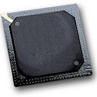
MPC564CZP40 Freescale Semiconductor, MPC564CZP40 Datasheet - Page 90

MPC564CZP40
Manufacturer Part Number
MPC564CZP40
Description
IC MPU 32BIT W/CODE COMP 388PBGA
Manufacturer
Freescale Semiconductor
Series
MPC5xxr
Specifications of MPC564CZP40
Core Processor
PowerPC
Core Size
32-Bit
Speed
40MHz
Connectivity
CAN, EBI/EMI, SCI, SPI, UART/USART
Peripherals
POR, PWM, WDT
Number Of I /o
56
Program Memory Size
512KB (512K x 8)
Program Memory Type
FLASH
Ram Size
32K x 8
Voltage - Supply (vcc/vdd)
2.5 V ~ 2.7 V
Data Converters
A/D 32x10b
Oscillator Type
External
Operating Temperature
-40°C ~ 85°C
Package / Case
388-BGA
Processor Series
MPC5xx
Core
PowerPC
Data Bus Width
32 bit
Data Ram Size
32 KB
Interface Type
CAN, JTAG, QSPI, SCI, SPI, UART
Maximum Clock Frequency
40 MHz
Number Of Programmable I/os
56
Number Of Timers
2
Operating Supply Voltage
0 V to 5 V
Maximum Operating Temperature
+ 85 C
Mounting Style
SMD/SMT
Minimum Operating Temperature
- 40 C
On-chip Adc
2 (10 bit, 32 Channel)
For Use With
MPC564EVB - KIT EVAL FOR MPC561/562/563/564
Lead Free Status / RoHS Status
Contains lead / RoHS non-compliant
Eeprom Size
-
Lead Free Status / Rohs Status
No
Available stocks
Company
Part Number
Manufacturer
Quantity
Price
Company:
Part Number:
MPC564CZP40
Manufacturer:
Freescale Semiconductor
Quantity:
10 000
- Current page: 90 of 1420
- Download datasheet (11Mb)
Overview
1.3.1.7
1.3.1.8
1.3.2
1.3.3
1.3.3.1
1.3.3.2
1-6
•
•
•
•
•
•
•
•
•
•
•
•
•
•
•
•
•
•
•
•
•
•
•
•
Composed of one 32-Kbyte CALRAM module
— 28-Kbyte static RAM
— 4-Kbyte calibration (overlay) RAM feature that allows calibration of Flash-based constants
Eight 512-byte overlay regions
One clock fast accesses
Two clock cycle access option for power saving
Standby power supply (IRAMSTBY) for data retention
24 address signals and 32 data signals can be used for general-purpose I/O in single-chip mode
16 GPIO in MIOS14
Many peripheral signals can be used as GPIO when not used as primary functions
5-V outputs with slew rate control
Compliant with Class 3 of the IEEE-ISTO 5001-1999
Program trace via branch trace messaging (BTM)
Data trace via data write messaging (DWM) and data read messaging (DRM)
Ownership trace via ownership trace messaging (OTM)
Run-time access to on-chip memory map and special-purpose registers (SPRs) via the READI
read/write access protocol
Watchpoint messaging via the auxiliary port
9 or 16 full-duplex auxiliary pin interface for medium and high visibility throughput
All features configurable and controllable via the auxiliary port
Supports the RCPU debug mode via the auxiliary port
True 5 V I/O
Two time processing units (TPU3) with 16 channels each
Each TPU3 is a micro-coded timer subsystem
8 Kbytes of dual port TPU RAM (DPTRAM) shared by two TPU3 modules for TPU micro-code
Six modulus counter sub-modules (MCSM)
10 double-action sub-modules (DASM)
Nexus Debug Port (Class 3)
Integrated I/O System
32-Kbyte Static RAM (CALRAM)
General Purpose I/O Support (GPIO)
Two Time Processor Units (TPU3)
22-Channel Modular I/O System (MIOS14)
MPC561/MPC563 Reference Manual, Rev. 1.2
Freescale Semiconductor
Related parts for MPC564CZP40
Image
Part Number
Description
Manufacturer
Datasheet
Request
R

Part Number:
Description:
MPC5 1K0 5%
Manufacturer:
TE Connectivity
Datasheet:

Part Number:
Description:
MPC5 500R 5%
Manufacturer:
TE Connectivity
Datasheet:

Part Number:
Description:
MPC5 5K0 5%
Manufacturer:
Tyco Electronics
Datasheet:

Part Number:
Description:
MPC5 5R0 5%
Manufacturer:
Tyco Electronics
Datasheet:

Part Number:
Description:
MPC5 50K 5%
Manufacturer:
Tyco Electronics
Datasheet:

Part Number:
Description:
MPC5 1R0 5%
Manufacturer:
Tyco Electronics
Datasheet:
Part Number:
Description:
Manufacturer:
Freescale Semiconductor, Inc
Datasheet:
Part Number:
Description:
Manufacturer:
Freescale Semiconductor, Inc
Datasheet:
Part Number:
Description:
Manufacturer:
Freescale Semiconductor, Inc
Datasheet:
Part Number:
Description:
Manufacturer:
Freescale Semiconductor, Inc
Datasheet:
Part Number:
Description:
Manufacturer:
Freescale Semiconductor, Inc
Datasheet:


