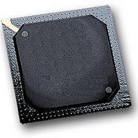
MPC564CZP40 Freescale Semiconductor, MPC564CZP40 Datasheet - Page 1218

MPC564CZP40
Manufacturer Part Number
MPC564CZP40
Description
IC MPU 32BIT W/CODE COMP 388PBGA
Manufacturer
Freescale Semiconductor
Series
MPC5xxr
Specifications of MPC564CZP40
Core Processor
PowerPC
Core Size
32-Bit
Speed
40MHz
Connectivity
CAN, EBI/EMI, SCI, SPI, UART/USART
Peripherals
POR, PWM, WDT
Number Of I /o
56
Program Memory Size
512KB (512K x 8)
Program Memory Type
FLASH
Ram Size
32K x 8
Voltage - Supply (vcc/vdd)
2.5 V ~ 2.7 V
Data Converters
A/D 32x10b
Oscillator Type
External
Operating Temperature
-40°C ~ 85°C
Package / Case
388-BGA
Processor Series
MPC5xx
Core
PowerPC
Data Bus Width
32 bit
Data Ram Size
32 KB
Interface Type
CAN, JTAG, QSPI, SCI, SPI, UART
Maximum Clock Frequency
40 MHz
Number Of Programmable I/os
56
Number Of Timers
2
Operating Supply Voltage
0 V to 5 V
Maximum Operating Temperature
+ 85 C
Mounting Style
SMD/SMT
Minimum Operating Temperature
- 40 C
On-chip Adc
2 (10 bit, 32 Channel)
For Use With
MPC564EVB - KIT EVAL FOR MPC561/562/563/564
Lead Free Status / RoHS Status
Contains lead / RoHS non-compliant
Eeprom Size
-
Lead Free Status / Rohs Status
No
Available stocks
Company
Part Number
Manufacturer
Quantity
Price
Company:
Part Number:
MPC564CZP40
Manufacturer:
Freescale Semiconductor
Quantity:
10 000
- Current page: 1218 of 1420
- Download datasheet (11Mb)
Electrical Characteristics
Functional operating conditions are given in
maximum ratings are stress ratings only, and functional operation at the maximum is not guaranteed. Stress
beyond those listed may affect device reliability or cause permanent damage to the device.
This device contains circuitry protecting against damage due to high static voltage or electrical fields;
however, it is advised that normal precautions be taken to avoid application of any voltages higher than
maximum-rated voltages to this high-impedance circuit. Reliability of operation is enhanced if unused
inputs are tied to an appropriate logic voltage level (e.g., either V
F.1
The MPC561/MPC563 is available in packaged form. The package is a 388-ball PBGA having a 1.0 mm
ball pitch, Freescale case outline 1164-01 (See
F.2
F.2.1
The document referenced for the EMC testing of MPC561/MPC563 is SAE J1752/3 Issued 1995-03
F-2
1
2
3
4
5
6
7
8
9
10
11
12
13
14
15
16
For internal digital supply of V
2.6 volt supply pins can withstand up to 3.6 volts for acumulative time of 24 hours over the lifetime of the device.
During operation the value of V
These power supplies are available on MPC563 and MPC564 only.
Maximum average current into the IRAMSTBY pin must be < 1.75mA.
V
All 2.6-V input-only pins are 5-V tolerant.
Note that long term reliability may be compromised if 2.6-V output drivers drive a node which has been previously
pulled to >3.1 V by an external component. HRESET and SRESET are fully 5-V compatible.
6.35 V on 5-V only pins (all QADC, all TPU, all QSMCM and the following MIOS pins: MDA[11:15], MDA[27:31],
MPWM16, MPIO32B[7:9]/MPWM[20:21], MPIO32B11/C_CNRX0, MPIO32B12/C_CNTX0 ). Internal structures hold
the input voltage below this maximum voltage on all of these pins, except the QSMCM RXD1/QPI1 and
RXD2/QPI2/C_CNRX0 pins, if the maximum injection current specification is met (1 mA for all pins; exception: 3 mA
on QADC pins) and VDDH is within Operating Voltage specifications (see specification 43 in
The RXD1/QGPI1 and RXD2/GPI2 pins do not have clamp diodes to VDDH. Voltage must be limited to less than 6.5
volts on these 2 pins to prevent damage.
Maximum continuous current on I/O pins provided the overall power dissipation is below the power dissipation of the
package. Proper operation is not guaranteed at this condition.
Condition applies to one pin at a time.
Transitions within the limit do not affect device reliability or cause permanent damage. Exceeding limit may cause
permanent conversion error on stressed channels and on unstressed channels.
Maximum transient current per ISO7637.
Maximum operating temperature on any solder ball in outer four rows of solder balls on the package. These rows are
referred to as “Perimeter Balls” to distinguish them from the balls in the center of the package.
Solder profile per CDF-AEC-Q100, current revision.
Moisture sensitivity per JEDEC test method J-STD-020-A (April 1999).
DDA
Package
EMI Characteristics
=5.0 V
Reference Documents
Negative current flows out of the pin and positive current flows into the pin.
±
5%.
DDL
FLASH
MPC561/MPC563 Reference Manual, Rev. 1.2
= 2.6-V typical.
must be 5.0 V
Section F.5, “DC Electrical
Figure F-64
NOTE
±
5%
and
Figure
SS
or V
F-65).
DD
Characteristics.” Absolute
).
Table
Freescale Semiconductor
F-4). Exception:
Related parts for MPC564CZP40
Image
Part Number
Description
Manufacturer
Datasheet
Request
R

Part Number:
Description:
MPC5 1K0 5%
Manufacturer:
TE Connectivity
Datasheet:

Part Number:
Description:
MPC5 500R 5%
Manufacturer:
TE Connectivity
Datasheet:

Part Number:
Description:
MPC5 5K0 5%
Manufacturer:
Tyco Electronics
Datasheet:

Part Number:
Description:
MPC5 5R0 5%
Manufacturer:
Tyco Electronics
Datasheet:

Part Number:
Description:
MPC5 50K 5%
Manufacturer:
Tyco Electronics
Datasheet:

Part Number:
Description:
MPC5 1R0 5%
Manufacturer:
Tyco Electronics
Datasheet:
Part Number:
Description:
Manufacturer:
Freescale Semiconductor, Inc
Datasheet:
Part Number:
Description:
Manufacturer:
Freescale Semiconductor, Inc
Datasheet:
Part Number:
Description:
Manufacturer:
Freescale Semiconductor, Inc
Datasheet:
Part Number:
Description:
Manufacturer:
Freescale Semiconductor, Inc
Datasheet:
Part Number:
Description:
Manufacturer:
Freescale Semiconductor, Inc
Datasheet:


