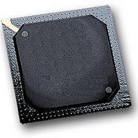
MPC564CZP40 Freescale Semiconductor, MPC564CZP40 Datasheet - Page 642

MPC564CZP40
Manufacturer Part Number
MPC564CZP40
Description
IC MPU 32BIT W/CODE COMP 388PBGA
Manufacturer
Freescale Semiconductor
Series
MPC5xxr
Specifications of MPC564CZP40
Core Processor
PowerPC
Core Size
32-Bit
Speed
40MHz
Connectivity
CAN, EBI/EMI, SCI, SPI, UART/USART
Peripherals
POR, PWM, WDT
Number Of I /o
56
Program Memory Size
512KB (512K x 8)
Program Memory Type
FLASH
Ram Size
32K x 8
Voltage - Supply (vcc/vdd)
2.5 V ~ 2.7 V
Data Converters
A/D 32x10b
Oscillator Type
External
Operating Temperature
-40°C ~ 85°C
Package / Case
388-BGA
Processor Series
MPC5xx
Core
PowerPC
Data Bus Width
32 bit
Data Ram Size
32 KB
Interface Type
CAN, JTAG, QSPI, SCI, SPI, UART
Maximum Clock Frequency
40 MHz
Number Of Programmable I/os
56
Number Of Timers
2
Operating Supply Voltage
0 V to 5 V
Maximum Operating Temperature
+ 85 C
Mounting Style
SMD/SMT
Minimum Operating Temperature
- 40 C
On-chip Adc
2 (10 bit, 32 Channel)
For Use With
MPC564EVB - KIT EVAL FOR MPC561/562/563/564
Lead Free Status / RoHS Status
Contains lead / RoHS non-compliant
Eeprom Size
-
Lead Free Status / Rohs Status
No
Available stocks
Company
Part Number
Manufacturer
Quantity
Price
Company:
Part Number:
MPC564CZP40
Manufacturer:
Freescale Semiconductor
Quantity:
10 000
- Current page: 642 of 1420
- Download datasheet (11Mb)
Queued Serial Multi-Channel Module
Refer to
15.6.3
Seven pins are associated with the QSPI. When not needed by the QSPI, they can be configured for
general-purpose I/O.
determines whether the pins are designated as input or output. The user must initialize DDRQS for the
QSPI to function correctly.
15-24
Bits
4:7
0
1
2
3
The PCS0 bit represents the dual-function PCS0/SS.
1
PCS[3:0] Peripheral chip selects. Use peripheral chip-select bits to select an external device for serial data transfer. More
CONT
CONT
BITSE
Name
CONT
DSCK
MSB
DT
Section 15.6.5, “Master Mode
—
0
QSPI Pins
Continue
0 Control of chip selects returned to PORTQS after transfer is complete.
1 Peripheral chip selects remain asserted after transfer is complete.
Bits per transfer enable
0 Eight bits
1 Number of bits set in BITS field of SPCR0.
Delay after transfer
0 Delay after transfer is 17 ÷ f
1 SPCR1 DTL[7:0] specifies delay after transfer PCS valid to SCK.
PCS to SCK Delay
0 PCS valid to SCK delay is one-half SCK.
1 SPCR1 DSCKL[6:0] specifies delay from PCS valid to SCK.
than one peripheral chip select may be activated at a time, and more than one peripheral chip can be connected
to each PCS pin, provided proper fanout is observed. PCS0 shares a pin with the slave select (SS) signal, which
initiates slave mode serial transfer. If SS is taken low when the QSPI is in master mode, a mode fault occurs.
BITSE
BITSE
Command Control
—
Table 15-20
1
Figure 15-17. CR[0:F] — Command RAM 0x30 51C0, 0x30 51DF
Table 15-19. Command RAM Bit Descriptions
MPC561/MPC563 Reference Manual, Rev. 1.2
DT
DT
—
2
identifies the QSPI pins and their functions. Register DDRQS
Operation” for more information on the command RAM.
SYS
.
DSCK
DSCK
—
3
Description
PCS3
PCS3
—
4
Peripheral Chip Select
PCS2
PCS2
—
5
PCS1
PCS1
—
6
Freescale Semiconductor
PCS0
PCS0
LSB
—
7
1
1
Related parts for MPC564CZP40
Image
Part Number
Description
Manufacturer
Datasheet
Request
R

Part Number:
Description:
MPC5 1K0 5%
Manufacturer:
TE Connectivity
Datasheet:

Part Number:
Description:
MPC5 500R 5%
Manufacturer:
TE Connectivity
Datasheet:

Part Number:
Description:
MPC5 5K0 5%
Manufacturer:
Tyco Electronics
Datasheet:

Part Number:
Description:
MPC5 5R0 5%
Manufacturer:
Tyco Electronics
Datasheet:

Part Number:
Description:
MPC5 50K 5%
Manufacturer:
Tyco Electronics
Datasheet:

Part Number:
Description:
MPC5 1R0 5%
Manufacturer:
Tyco Electronics
Datasheet:
Part Number:
Description:
Manufacturer:
Freescale Semiconductor, Inc
Datasheet:
Part Number:
Description:
Manufacturer:
Freescale Semiconductor, Inc
Datasheet:
Part Number:
Description:
Manufacturer:
Freescale Semiconductor, Inc
Datasheet:
Part Number:
Description:
Manufacturer:
Freescale Semiconductor, Inc
Datasheet:
Part Number:
Description:
Manufacturer:
Freescale Semiconductor, Inc
Datasheet:


