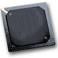
MPC564CZP40 Freescale Semiconductor, MPC564CZP40 Datasheet - Page 312

MPC564CZP40
Manufacturer Part Number
MPC564CZP40
Description
IC MPU 32BIT W/CODE COMP 388PBGA
Manufacturer
Freescale Semiconductor
Series
MPC5xxr
Specifications of MPC564CZP40
Core Processor
PowerPC
Core Size
32-Bit
Speed
40MHz
Connectivity
CAN, EBI/EMI, SCI, SPI, UART/USART
Peripherals
POR, PWM, WDT
Number Of I /o
56
Program Memory Size
512KB (512K x 8)
Program Memory Type
FLASH
Ram Size
32K x 8
Voltage - Supply (vcc/vdd)
2.5 V ~ 2.7 V
Data Converters
A/D 32x10b
Oscillator Type
External
Operating Temperature
-40°C ~ 85°C
Package / Case
388-BGA
Processor Series
MPC5xx
Core
PowerPC
Data Bus Width
32 bit
Data Ram Size
32 KB
Interface Type
CAN, JTAG, QSPI, SCI, SPI, UART
Maximum Clock Frequency
40 MHz
Number Of Programmable I/os
56
Number Of Timers
2
Operating Supply Voltage
0 V to 5 V
Maximum Operating Temperature
+ 85 C
Mounting Style
SMD/SMT
Minimum Operating Temperature
- 40 C
On-chip Adc
2 (10 bit, 32 Channel)
For Use With
MPC564EVB - KIT EVAL FOR MPC561/562/563/564
Lead Free Status / RoHS Status
Contains lead / RoHS non-compliant
Eeprom Size
-
Lead Free Status / Rohs Status
No
Available stocks
Company
Part Number
Manufacturer
Quantity
Price
Company:
Part Number:
MPC564CZP40
Manufacturer:
Freescale Semiconductor
Quantity:
10 000
- Current page: 312 of 1420
- Download datasheet (11Mb)
Clocks and Power Control
The values of the PITRTCLK clock division and TMBCLK clock division can be changed by software.
The RTDIV bit value in the SCCR register defines the division of PITRTCLK. All possible combinations
of the TMBCLK divisions are listed in
8.5.1
The general system clocks (GCLK1C, GCLK2C, GCLK1, GCLK2, GCLK1_50, and GCLK2_50) are the
basic clock supplied to all modules and sub-modules on the MPC561/MPC563. GCLK1C and GCLK2C
are supplied to the RCPU and to the BBC. GCLK1C and GCLK2C are stopped when the chip enters the
doze-low power mode. GCLK1 and GCLK2 are supplied to the SIU and the clock module. The external
bus clock GCLK2_50 is the same as CLKOUT. The general system clock defaults to VCO/2 = 20 MHz
(assuming a 20-MHz system frequency) with default power-on reset MF values.
8-10
1
MODCK[1:3]
indicates MODCK pins value during power-on reset
100
101
110
111
General System Clocks
The reset value of the PLL pre-divider is one.
1
LME
1
0
0
1
To ensure correct operation of the time base, keep the system clock to time
base clock ratio above 4 and always set SCCR[TBS] = 1 when running on
the backup clock (limp mode).
Table 8-1. Reset Clocks Source Configuration (continued)
SCCR[TBS]
RTSEL
1
1
1
1
0
0
Default Values after PORESET
MPC561/MPC563 Reference Manual, Rev. 1.2
RTDIV
1
1
1
Table 8-2. TMBCLK Divisions
Table
MF + 1
8-2.
1
5
1
NOTE
MF + 1
1, 2
> 2
—
Division
PITCLK
256
256
256
TMBCLK
Division
1
16
16
4
TMBCLK
Division
16
16
4
Normal operation, PLL enabled.
1:1 Mode
Main timing reference is EXT-
CLK pin (>15MHz)
Limp mode disabled.
Normal operation, PLL enabled.
Main timing reference is EXT-
CLK (3-5 MHz).
Limp mode disabled.
Normal operation, PLL enabled.
1:1 Mode
Main timing reference is EXT-
CLK pin (>15MHz)
Limp mode enabled.
SPLL Options
Freescale Semiconductor
Related parts for MPC564CZP40
Image
Part Number
Description
Manufacturer
Datasheet
Request
R

Part Number:
Description:
MPC5 1K0 5%
Manufacturer:
TE Connectivity
Datasheet:

Part Number:
Description:
MPC5 500R 5%
Manufacturer:
TE Connectivity
Datasheet:

Part Number:
Description:
MPC5 5K0 5%
Manufacturer:
Tyco Electronics
Datasheet:

Part Number:
Description:
MPC5 5R0 5%
Manufacturer:
Tyco Electronics
Datasheet:

Part Number:
Description:
MPC5 50K 5%
Manufacturer:
Tyco Electronics
Datasheet:

Part Number:
Description:
MPC5 1R0 5%
Manufacturer:
Tyco Electronics
Datasheet:
Part Number:
Description:
Manufacturer:
Freescale Semiconductor, Inc
Datasheet:
Part Number:
Description:
Manufacturer:
Freescale Semiconductor, Inc
Datasheet:
Part Number:
Description:
Manufacturer:
Freescale Semiconductor, Inc
Datasheet:
Part Number:
Description:
Manufacturer:
Freescale Semiconductor, Inc
Datasheet:
Part Number:
Description:
Manufacturer:
Freescale Semiconductor, Inc
Datasheet:


