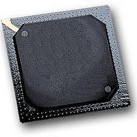
MPC564CZP40 Freescale Semiconductor, MPC564CZP40 Datasheet - Page 380

MPC564CZP40
Manufacturer Part Number
MPC564CZP40
Description
IC MPU 32BIT W/CODE COMP 388PBGA
Manufacturer
Freescale Semiconductor
Series
MPC5xxr
Specifications of MPC564CZP40
Core Processor
PowerPC
Core Size
32-Bit
Speed
40MHz
Connectivity
CAN, EBI/EMI, SCI, SPI, UART/USART
Peripherals
POR, PWM, WDT
Number Of I /o
56
Program Memory Size
512KB (512K x 8)
Program Memory Type
FLASH
Ram Size
32K x 8
Voltage - Supply (vcc/vdd)
2.5 V ~ 2.7 V
Data Converters
A/D 32x10b
Oscillator Type
External
Operating Temperature
-40°C ~ 85°C
Package / Case
388-BGA
Processor Series
MPC5xx
Core
PowerPC
Data Bus Width
32 bit
Data Ram Size
32 KB
Interface Type
CAN, JTAG, QSPI, SCI, SPI, UART
Maximum Clock Frequency
40 MHz
Number Of Programmable I/os
56
Number Of Timers
2
Operating Supply Voltage
0 V to 5 V
Maximum Operating Temperature
+ 85 C
Mounting Style
SMD/SMT
Minimum Operating Temperature
- 40 C
On-chip Adc
2 (10 bit, 32 Channel)
For Use With
MPC564EVB - KIT EVAL FOR MPC561/562/563/564
Lead Free Status / RoHS Status
Contains lead / RoHS non-compliant
Eeprom Size
-
Lead Free Status / Rohs Status
No
Available stocks
Company
Part Number
Manufacturer
Quantity
Price
Company:
Part Number:
MPC564CZP40
Manufacturer:
Freescale Semiconductor
Quantity:
10 000
- Current page: 380 of 1420
- Download datasheet (11Mb)
External Bus Interface
9.5.8.7
This signal is sent from the master to the slave to indicate that there is a data beat following the current
data beat. The master uses this signal to give the slave advance warning of the remaining data in the burst.
BDIP can also be used to terminate the burst cycle early. Refer to
Section 9.5.5, “Burst
Base Registers
9.5.9
The EBI uses three termination signals:
9.5.9.1
Transfer acknowledge (TA) indicates normal completion of the bus transfer. During a burst cycle, the slave
asserts this signal with every data beat returned or accepted.
9.5.9.2
A slave sends the BI signal to the master to indicate that the addressed device does not have burst
capability. If this signal is asserted, the master must transfer in multiple cycles and increment the address
for the slave to complete the burst transfer. For a system that does not use the burst mode at all, this signal
can be tied low permanently. Refer to
for BI options.
9.5.9.3
The TEA signal terminates a bus cycle under one or more bus error conditions. The current bus cycle must
be aborted. This signal overrides any other cycle termination signals, such as transfer acknowledge.
9.5.9.4
The transfer protocol was defined to avoid electrical contention on lines that can be driven by various
sources. To this end, a slave must not drive signals associated with the data transfer until the address phase
is completed and it recognizes the address as its own. The slave must disconnect from signals immediately
after it has acknowledged the cycle and no later than the termination of the next address phase cycle. This
means that the termination signals must be connected to power through a pull-up resistor to avoid the
situation in which a master samples an undefined value in any of these signals when no real slave is
addressed.
9-40
Refer to
1
•
•
•
Cases in which both TS and STS are asserted indicate normal cycles with the show cycle attribute.
Transfer acknowledge (TA)
Burst inhibit (BI)
Transfer error acknowledge (TEA)
Figure 9-28
Termination Signals
Burst Data in Progress
Transfer Acknowledge
Burst Inhibit
Transfer Error Acknowledge
Termination Signals Protocol
(BR0–BR3)” for memory controller BDIP options.
Mechanism” for more information. Refer to
and
Figure
MPC561/MPC563 Reference Manual, Rev. 1.2
9-29.
Section 10.9.3, “Memory Controller Base Registers
Section 9.5.4, “Burst
Section 10.9.3, “Memory Controller
Freescale Semiconductor
Transfer” and
(BR0–BR3)”
Related parts for MPC564CZP40
Image
Part Number
Description
Manufacturer
Datasheet
Request
R

Part Number:
Description:
MPC5 1K0 5%
Manufacturer:
TE Connectivity
Datasheet:

Part Number:
Description:
MPC5 500R 5%
Manufacturer:
TE Connectivity
Datasheet:

Part Number:
Description:
MPC5 5K0 5%
Manufacturer:
Tyco Electronics
Datasheet:

Part Number:
Description:
MPC5 5R0 5%
Manufacturer:
Tyco Electronics
Datasheet:

Part Number:
Description:
MPC5 50K 5%
Manufacturer:
Tyco Electronics
Datasheet:

Part Number:
Description:
MPC5 1R0 5%
Manufacturer:
Tyco Electronics
Datasheet:
Part Number:
Description:
Manufacturer:
Freescale Semiconductor, Inc
Datasheet:
Part Number:
Description:
Manufacturer:
Freescale Semiconductor, Inc
Datasheet:
Part Number:
Description:
Manufacturer:
Freescale Semiconductor, Inc
Datasheet:
Part Number:
Description:
Manufacturer:
Freescale Semiconductor, Inc
Datasheet:
Part Number:
Description:
Manufacturer:
Freescale Semiconductor, Inc
Datasheet:


