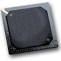
MPC564CZP40 Freescale Semiconductor, MPC564CZP40 Datasheet - Page 203

MPC564CZP40
Manufacturer Part Number
MPC564CZP40
Description
IC MPU 32BIT W/CODE COMP 388PBGA
Manufacturer
Freescale Semiconductor
Series
MPC5xxr
Specifications of MPC564CZP40
Core Processor
PowerPC
Core Size
32-Bit
Speed
40MHz
Connectivity
CAN, EBI/EMI, SCI, SPI, UART/USART
Peripherals
POR, PWM, WDT
Number Of I /o
56
Program Memory Size
512KB (512K x 8)
Program Memory Type
FLASH
Ram Size
32K x 8
Voltage - Supply (vcc/vdd)
2.5 V ~ 2.7 V
Data Converters
A/D 32x10b
Oscillator Type
External
Operating Temperature
-40°C ~ 85°C
Package / Case
388-BGA
Processor Series
MPC5xx
Core
PowerPC
Data Bus Width
32 bit
Data Ram Size
32 KB
Interface Type
CAN, JTAG, QSPI, SCI, SPI, UART
Maximum Clock Frequency
40 MHz
Number Of Programmable I/os
56
Number Of Timers
2
Operating Supply Voltage
0 V to 5 V
Maximum Operating Temperature
+ 85 C
Mounting Style
SMD/SMT
Minimum Operating Temperature
- 40 C
On-chip Adc
2 (10 bit, 32 Channel)
For Use With
MPC564EVB - KIT EVAL FOR MPC561/562/563/564
Lead Free Status / RoHS Status
Contains lead / RoHS non-compliant
Eeprom Size
-
Lead Free Status / Rohs Status
No
Available stocks
Company
Part Number
Manufacturer
Quantity
Price
Company:
Part Number:
MPC564CZP40
Manufacturer:
Freescale Semiconductor
Quantity:
10 000
- Current page: 203 of 1420
- Download datasheet (11Mb)
See
When a data protection error exception is taken, instruction execution resumes at offset 0x1400 from the
base address indicated by MSR[IP].
3.15.4.16 Implementation-Dependent Debug Exceptions
Implementation-dependent debug exceptions occur in the following cases:
See
Freescale Semiconductor
1
•
•
•
Table 3-36
Table 3-37
Save/Restore Register 0 (SRR0)
Save/Restore Register 1 (SRR1)
If the exception occurs during a data access in Decompression On mode, the SRR0 register will contain the address
of the Load/Store instruction in compressed format.
Machine State Register (MSR)
Data Address Register (DAR)
Data/Storage Interrupt Status
When there is an internal breakpoint match (for more details, refer to
Support.”
When a peripheral breakpoint request is asserted to the RCPU.
When the development port request is asserted to the RCPU. Refer to
Support,” for details on how to generate the development port-interrupt request.
Register (DSISR)
Register Name
for data-protection-error exception register settings.
for debug-exception register settings.
Table 3-36. Register Settings Following a Data Protection Error Exception
1
MPC561/MPC563 Reference Manual, Rev. 1.2
DCMPEN
Other
Other
Bits
0:15
7:31
ME
0:3
LE
All
All
IP
4
5
6
Set to the effective address of the instruction that caused the
exception
implementation, bit 30 of the SRR1 is never cleared, except by
loading a zero value from MSR[RI]
No change
Bit is copied from ILE
This bit is set according to (BBCMCR[EN_COMP] AND
BBCMCR[EXC_COMP])
Cleared to 0
Set to 1 if the storage access is not permitted by the protection
mechanism. Otherwise cleared to 0
Cleared to 0
Set to 1 for a store operation and cleared to 0 for a load
operation
Cleared to 0
exception
Cleared to 0
Loaded from bits [16:31] of MSR. In the current
No change
Cleared to 0
Set to the effective address of the data access that caused the
Description
Chapter 23, “Development
Chapter 23, “Development
Central Processing Unit
3-59
Related parts for MPC564CZP40
Image
Part Number
Description
Manufacturer
Datasheet
Request
R

Part Number:
Description:
MPC5 1K0 5%
Manufacturer:
TE Connectivity
Datasheet:

Part Number:
Description:
MPC5 500R 5%
Manufacturer:
TE Connectivity
Datasheet:

Part Number:
Description:
MPC5 5K0 5%
Manufacturer:
Tyco Electronics
Datasheet:

Part Number:
Description:
MPC5 5R0 5%
Manufacturer:
Tyco Electronics
Datasheet:

Part Number:
Description:
MPC5 50K 5%
Manufacturer:
Tyco Electronics
Datasheet:

Part Number:
Description:
MPC5 1R0 5%
Manufacturer:
Tyco Electronics
Datasheet:
Part Number:
Description:
Manufacturer:
Freescale Semiconductor, Inc
Datasheet:
Part Number:
Description:
Manufacturer:
Freescale Semiconductor, Inc
Datasheet:
Part Number:
Description:
Manufacturer:
Freescale Semiconductor, Inc
Datasheet:
Part Number:
Description:
Manufacturer:
Freescale Semiconductor, Inc
Datasheet:
Part Number:
Description:
Manufacturer:
Freescale Semiconductor, Inc
Datasheet:


