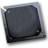
MPC564CZP40 Freescale Semiconductor, MPC564CZP40 Datasheet - Page 746

MPC564CZP40
Manufacturer Part Number
MPC564CZP40
Description
IC MPU 32BIT W/CODE COMP 388PBGA
Manufacturer
Freescale Semiconductor
Series
MPC5xxr
Specifications of MPC564CZP40
Core Processor
PowerPC
Core Size
32-Bit
Speed
40MHz
Connectivity
CAN, EBI/EMI, SCI, SPI, UART/USART
Peripherals
POR, PWM, WDT
Number Of I /o
56
Program Memory Size
512KB (512K x 8)
Program Memory Type
FLASH
Ram Size
32K x 8
Voltage - Supply (vcc/vdd)
2.5 V ~ 2.7 V
Data Converters
A/D 32x10b
Oscillator Type
External
Operating Temperature
-40°C ~ 85°C
Package / Case
388-BGA
Processor Series
MPC5xx
Core
PowerPC
Data Bus Width
32 bit
Data Ram Size
32 KB
Interface Type
CAN, JTAG, QSPI, SCI, SPI, UART
Maximum Clock Frequency
40 MHz
Number Of Programmable I/os
56
Number Of Timers
2
Operating Supply Voltage
0 V to 5 V
Maximum Operating Temperature
+ 85 C
Mounting Style
SMD/SMT
Minimum Operating Temperature
- 40 C
On-chip Adc
2 (10 bit, 32 Channel)
For Use With
MPC564EVB - KIT EVAL FOR MPC561/562/563/564
Lead Free Status / RoHS Status
Contains lead / RoHS non-compliant
Eeprom Size
-
Lead Free Status / Rohs Status
No
Available stocks
Company
Part Number
Manufacturer
Quantity
Price
Company:
Part Number:
MPC564CZP40
Manufacturer:
Freescale Semiconductor
Quantity:
10 000
- Current page: 746 of 1420
- Download datasheet (11Mb)
Modular Input/Output Subsystem (MIOS14)
17.6.1.2
This register is reserved and is shown for information purposes only.
17.6.1.3
This read-only register contains the hard-coded values of the module and version number.
17-14
1
SRESET
This field contains the revision level of the MIOS module and may change with different revisions of the device.
SRESET
Bits
1:13
14
15
Reset
0
Field
Addr
Field TEST
Addr
Field
Addr
MSB
Name
TEST
VFLS
MSB
0
MIOS14 Vector Register (MIOS14VECT)
MIOS14 Module and Version Number Register (MIOS14VNR)
VF
MSB
—
0
0
1
Figure 17-6. MIOS14 Module/Version Number Register (MIOS14VNR)
Test — This bit is used for MIOS14 factory testing and should always be programmed to a 0.
Reserved
VF Pin Multiplex — This bit controls the function of the VF pins (VF0/MPIO32B0, VF1/MPIO32B1,
VF2/MPIO32B2)
0 = MIOS14 General-Purpose I/O is selected (MPIO32B0, MPIO32B1, MPIO32B2)
1 = VF function is selected (VF[0:2])
VFLS Pin Multiplex — This bit controls the function of the VFLS signals (VFLS0/MPIO32B3,
VFLS1/MPIO32B4)
0 = MIOS14 General-Purpose I/O is selected (MPIO32B3, MPIO32B4)
1 = VFLS function is selected (VFLS[0:1])
1
1
Figure 17-4. Test and Signal Control Register (MIOS14TPCR)
2
2
2
3
3
Figure 17-5. Vector Register (MIOS14VECT)
3
Table 17-3. MIOS14TPCR Bit Descriptions
MN
MPC561/MPC563 Reference Manual, Rev. 1.2
—
4
4
4
5
5
5
6
0000_0000_0000_0000
0000_0000_0000_0000
6
6
7
Unaffected
0x30 6804
0x30 6800
—
0x30 6802
7
7
8
Description
8
8
9
9
10
9
VECT
10
11
10
11
12
11
VN
1
12
12
Freescale Semiconductor
13
13
13
—
VF
14
14
14
VFLS
LSB
15
LSB
LSB
15
15
Related parts for MPC564CZP40
Image
Part Number
Description
Manufacturer
Datasheet
Request
R

Part Number:
Description:
MPC5 1K0 5%
Manufacturer:
TE Connectivity
Datasheet:

Part Number:
Description:
MPC5 500R 5%
Manufacturer:
TE Connectivity
Datasheet:

Part Number:
Description:
MPC5 5K0 5%
Manufacturer:
Tyco Electronics
Datasheet:

Part Number:
Description:
MPC5 5R0 5%
Manufacturer:
Tyco Electronics
Datasheet:

Part Number:
Description:
MPC5 50K 5%
Manufacturer:
Tyco Electronics
Datasheet:

Part Number:
Description:
MPC5 1R0 5%
Manufacturer:
Tyco Electronics
Datasheet:
Part Number:
Description:
Manufacturer:
Freescale Semiconductor, Inc
Datasheet:
Part Number:
Description:
Manufacturer:
Freescale Semiconductor, Inc
Datasheet:
Part Number:
Description:
Manufacturer:
Freescale Semiconductor, Inc
Datasheet:
Part Number:
Description:
Manufacturer:
Freescale Semiconductor, Inc
Datasheet:
Part Number:
Description:
Manufacturer:
Freescale Semiconductor, Inc
Datasheet:


