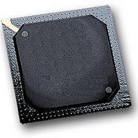
MPC564CZP40 Freescale Semiconductor, MPC564CZP40 Datasheet - Page 1151

MPC564CZP40
Manufacturer Part Number
MPC564CZP40
Description
IC MPU 32BIT W/CODE COMP 388PBGA
Manufacturer
Freescale Semiconductor
Series
MPC5xxr
Specifications of MPC564CZP40
Core Processor
PowerPC
Core Size
32-Bit
Speed
40MHz
Connectivity
CAN, EBI/EMI, SCI, SPI, UART/USART
Peripherals
POR, PWM, WDT
Number Of I /o
56
Program Memory Size
512KB (512K x 8)
Program Memory Type
FLASH
Ram Size
32K x 8
Voltage - Supply (vcc/vdd)
2.5 V ~ 2.7 V
Data Converters
A/D 32x10b
Oscillator Type
External
Operating Temperature
-40°C ~ 85°C
Package / Case
388-BGA
Processor Series
MPC5xx
Core
PowerPC
Data Bus Width
32 bit
Data Ram Size
32 KB
Interface Type
CAN, JTAG, QSPI, SCI, SPI, UART
Maximum Clock Frequency
40 MHz
Number Of Programmable I/os
56
Number Of Timers
2
Operating Supply Voltage
0 V to 5 V
Maximum Operating Temperature
+ 85 C
Mounting Style
SMD/SMT
Minimum Operating Temperature
- 40 C
On-chip Adc
2 (10 bit, 32 Channel)
For Use With
MPC564EVB - KIT EVAL FOR MPC561/562/563/564
Lead Free Status / RoHS Status
Contains lead / RoHS non-compliant
Eeprom Size
-
Lead Free Status / Rohs Status
No
Available stocks
Company
Part Number
Manufacturer
Quantity
Price
Company:
Part Number:
MPC564CZP40
Manufacturer:
Freescale Semiconductor
Quantity:
10 000
- Current page: 1151 of 1420
- Download datasheet (11Mb)
MF is the multiplication factor in the PLPRCR register (refer to
Reset-Control Register
C.3
C.3.1
Traces connecting capacitors, crystal, resistor should be as short as possible. Therefore, the components
(crystal, resistor and capacitors) should be placed as close to the oscillator pins of the MPC561/MPC563
as possible.
The voltage to the VDDSYN pin should be well regulated and the pin should be provided with an
extremely low impedance path from the VDDSYN filter to the VDDSYN pad.
The VSSSYN pin should be provided with an extremely low impedance path in the board. All the filters
for the supplies should be located as close as possible to the chip package. It is recommended to design
individual VSSSYN plane to improve VSSSYN quietness.
C.3.2
The traces from the oscillator pins and PLL pins of the MPC561/MPC563 should be guarded from all other
traces to reduce crosstalk. It can be provided by keeping other traces away from the oscillator circuit and
placing a ground plane around the components and traces.
C.3.3
IRAMSTBY is the data retention power supply for all on-board RAM arrays (CALRAM, DPTRAM,
DECRAM). It has a shunt regulator circuit to divert excess current to ground in order to regulate voltage
on the IRAMSTBY power supply pin. IRAMSTBY should be connected to a positive power supply, via a
resistor, and bypassed by a capacitor to ground as shown in
Freescale Semiconductor
PLL and Clock Oscillator External Components Layout
Requirements
Traces and Placement
Grounding/Guarding
IRAMSTBY Regulator Circuit
(PLPRCR)” for more information).
Figure C-8. PLL Off-Chip Capacitor Example
MPC561/MPC563 Reference Manual, Rev. 1.2
CXFC
Board
MPC56x Device
VDDSYN
XFC
Figure
Section 8.11.2, “PLL, Low-Power, and
C-9.
Clock and Board Guidelines
C-7
Related parts for MPC564CZP40
Image
Part Number
Description
Manufacturer
Datasheet
Request
R

Part Number:
Description:
MPC5 1K0 5%
Manufacturer:
TE Connectivity
Datasheet:

Part Number:
Description:
MPC5 500R 5%
Manufacturer:
TE Connectivity
Datasheet:

Part Number:
Description:
MPC5 5K0 5%
Manufacturer:
Tyco Electronics
Datasheet:

Part Number:
Description:
MPC5 5R0 5%
Manufacturer:
Tyco Electronics
Datasheet:

Part Number:
Description:
MPC5 50K 5%
Manufacturer:
Tyco Electronics
Datasheet:

Part Number:
Description:
MPC5 1R0 5%
Manufacturer:
Tyco Electronics
Datasheet:
Part Number:
Description:
Manufacturer:
Freescale Semiconductor, Inc
Datasheet:
Part Number:
Description:
Manufacturer:
Freescale Semiconductor, Inc
Datasheet:
Part Number:
Description:
Manufacturer:
Freescale Semiconductor, Inc
Datasheet:
Part Number:
Description:
Manufacturer:
Freescale Semiconductor, Inc
Datasheet:
Part Number:
Description:
Manufacturer:
Freescale Semiconductor, Inc
Datasheet:


