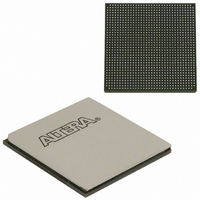
EP2SGX90EF1152C4N Altera, EP2SGX90EF1152C4N Datasheet - Page 117

EP2SGX90EF1152C4N
Manufacturer Part Number
EP2SGX90EF1152C4N
Description
IC STRATIX II GX 90K 1152-FBGA
Manufacturer
Altera
Series
Stratix® II GXr
Datasheet
1.EP2SGX30DF780C5.pdf
(316 pages)
Specifications of EP2SGX90EF1152C4N
Number Of Logic Elements/cells
90960
Number Of Labs/clbs
4548
Total Ram Bits
4520448
Number Of I /o
558
Voltage - Supply
1.15 V ~ 1.25 V
Mounting Type
Surface Mount
Operating Temperature
0°C ~ 70°C
Package / Case
1152-FBGA
Family Name
Stratix II GX
Number Of Logic Blocks/elements
90960
# I/os (max)
558
Frequency (max)
732.1MHz
Process Technology
SRAM
Operating Supply Voltage (typ)
1.2V
Logic Cells
90960
Ram Bits
4520448
Operating Supply Voltage (min)
1.15V
Operating Supply Voltage (max)
1.25V
Operating Temp Range
0C to 85C
Operating Temperature Classification
Commercial
Mounting
Surface Mount
Pin Count
1152
Package Type
FC-FBGA
For Use With
544-1725 - PCIE KIT W/S II GX EP2SGX90N544-1724 - SI KIT W/SII GX EP2SGX90N544-1702 - VIDEO KIT W/SII GX EP2SGX90N
Lead Free Status / RoHS Status
Lead free / RoHS Compliant
Number Of Gates
-
Lead Free Status / Rohs Status
Compliant
Other names
544-1767
EP2SGX90EF35C4NES
EP2SGX90EF35C4NES
Available stocks
Company
Part Number
Manufacturer
Quantity
Price
Company:
Part Number:
EP2SGX90EF1152C4N
Manufacturer:
ALTERA
Quantity:
648
- Current page: 117 of 316
- Download datasheet (2Mb)
Figure 2–74. Stratix II GX Enhanced PLL
Notes to
(1)
(2)
(3)
(4)
Altera Corporation
October 2007
Global or
Regional
Clock
INCLK[3..0]
Each clock source can come from any of the four clock pins that are physically located on the same side of the device
as the PLL.
If the feedback input is used, you will lose one (or two, if FBIN is differential) external clock output pin.
Each enhanced PLL has three differential external clock outputs or six single-ended external clock outputs.
The global or regional clock input can be driven by an output from another PLL, a pin-driven dedicated global or
regional clock, or through a clock control block provided the clock control block is fed by an output from another
PLL or a pin-driven dedicated global or regional clock. An internally generated global signal cannot drive the PLL.
Figure
4
Shaded Portions of the
PLL are Reconfigurable
2–74:
FBIN
Switchover
Circuitry
Clock
(2)
Enhanced PLLs
Stratix II GX devices contain up to four enhanced PLLs with advanced
clock management features. These features include support for external
clock feedback mode, spread-spectrum clocking, and counter cascading.
Figure 2–74
Fast PLLs
Stratix II GX devices contain up to four fast PLLs with high-speed serial
interfacing ability. The fast PLLs offer high-speed outputs to manage the
high-speed differential I/O interfaces.
the fast PLL.
/n
Phase Frequency
Detector
PFD
shows a diagram of the enhanced PLL.
Charge
Pump
Note (1)
Lock Detect
& Filter
Spectrum
/m
Spread
Loop
Filter
VCO Phase Selection
Affecting All Outputs
VCO Phase Selection
Selectable at Each
PLL Output Port
VCO
Stratix II GX Device Handbook, Volume 1
8
Figure 2–75
Post-Scale
Counters
/c0
/c1
/c2
/c3
/c4
/c5
From Adjacent PLL
6
Stratix II GX Architecture
shows a diagram of
4
8
6
Global
Clocks
Regional
Clocks
I/O Buffers (3)
to I/O or general
routing
2–109
Related parts for EP2SGX90EF1152C4N
Image
Part Number
Description
Manufacturer
Datasheet
Request
R

Part Number:
Description:
CYCLONE II STARTER KIT EP2C20N
Manufacturer:
Altera
Datasheet:

Part Number:
Description:
CPLD, EP610 Family, ECMOS Process, 300 Gates, 16 Macro Cells, 16 Reg., 16 User I/Os, 5V Supply, 35 Speed Grade, 24DIP
Manufacturer:
Altera Corporation
Datasheet:

Part Number:
Description:
CPLD, EP610 Family, ECMOS Process, 300 Gates, 16 Macro Cells, 16 Reg., 16 User I/Os, 5V Supply, 15 Speed Grade, 24DIP
Manufacturer:
Altera Corporation
Datasheet:

Part Number:
Description:
Manufacturer:
Altera Corporation
Datasheet:

Part Number:
Description:
CPLD, EP610 Family, ECMOS Process, 300 Gates, 16 Macro Cells, 16 Reg., 16 User I/Os, 5V Supply, 30 Speed Grade, 24DIP
Manufacturer:
Altera Corporation
Datasheet:

Part Number:
Description:
High-performance, low-power erasable programmable logic devices with 8 macrocells, 10ns
Manufacturer:
Altera Corporation
Datasheet:

Part Number:
Description:
High-performance, low-power erasable programmable logic devices with 8 macrocells, 7ns
Manufacturer:
Altera Corporation
Datasheet:

Part Number:
Description:
Classic EPLD
Manufacturer:
Altera Corporation
Datasheet:

Part Number:
Description:
High-performance, low-power erasable programmable logic devices with 8 macrocells, 10ns
Manufacturer:
Altera Corporation
Datasheet:

Part Number:
Description:
Manufacturer:
Altera Corporation
Datasheet:

Part Number:
Description:
Manufacturer:
Altera Corporation
Datasheet:

Part Number:
Description:
Manufacturer:
Altera Corporation
Datasheet:

Part Number:
Description:
CPLD, EP610 Family, ECMOS Process, 300 Gates, 16 Macro Cells, 16 Reg., 16 User I/Os, 5V Supply, 25 Speed Grade, 24DIP
Manufacturer:
Altera Corporation
Datasheet:


