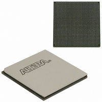
EP2SGX90EF1152C4N Altera, EP2SGX90EF1152C4N Datasheet - Page 139

EP2SGX90EF1152C4N
Manufacturer Part Number
EP2SGX90EF1152C4N
Description
IC STRATIX II GX 90K 1152-FBGA
Manufacturer
Altera
Series
Stratix® II GXr
Datasheet
1.EP2SGX30DF780C5.pdf
(316 pages)
Specifications of EP2SGX90EF1152C4N
Number Of Logic Elements/cells
90960
Number Of Labs/clbs
4548
Total Ram Bits
4520448
Number Of I /o
558
Voltage - Supply
1.15 V ~ 1.25 V
Mounting Type
Surface Mount
Operating Temperature
0°C ~ 70°C
Package / Case
1152-FBGA
Family Name
Stratix II GX
Number Of Logic Blocks/elements
90960
# I/os (max)
558
Frequency (max)
732.1MHz
Process Technology
SRAM
Operating Supply Voltage (typ)
1.2V
Logic Cells
90960
Ram Bits
4520448
Operating Supply Voltage (min)
1.15V
Operating Supply Voltage (max)
1.25V
Operating Temp Range
0C to 85C
Operating Temperature Classification
Commercial
Mounting
Surface Mount
Pin Count
1152
Package Type
FC-FBGA
For Use With
544-1725 - PCIE KIT W/S II GX EP2SGX90N544-1724 - SI KIT W/SII GX EP2SGX90N544-1702 - VIDEO KIT W/SII GX EP2SGX90N
Lead Free Status / RoHS Status
Lead free / RoHS Compliant
Number Of Gates
-
Lead Free Status / Rohs Status
Compliant
Other names
544-1767
EP2SGX90EF35C4NES
EP2SGX90EF35C4NES
Available stocks
Company
Part Number
Manufacturer
Quantity
Price
Company:
Part Number:
EP2SGX90EF1152C4N
Manufacturer:
ALTERA
Quantity:
648
- Current page: 139 of 316
- Download datasheet (2Mb)
Altera Corporation
October 2007
Note to
(1)
Series termination with
calibration
Differential termination
Table 2–34. On-Chip Termination Support by I/O Banks (Part 2 of 2)
On-Chip Termination Support
Clock pins CLK1 and CLK3, and pins FPLL[7..8]CLK do not support differential on-chip termination. Clock pins
CLK0 and CLK2, do support differential on-chip termination. Clock pins in the top and bottom banks (CLK[4..7,
12..15]) do not support differential on-chip termination.
Table
2–34:
f
(1)
Differential On-Chip Termination
Stratix II GX devices support internal differential termination with a
nominal resistance value of 100 for LVDS input receiver buffers. LVPECL
input signals (supported on clock pins only) require an external
termination resistor. Differential on-chip termination is supported across
the full range of supported differential data rates, as shown in the
High-Speed I/O Specifications section of the
chapter in volume 1 of the Stratix II GX Device Handbook.
For more information on differential on-chip termination, refer to the
High-Speed Differential I/O Interfaces with DPA in Stratix II & Stratix II GX
Devices
3.3-V LVTTL
3.3-V LVCMOS
2.5-V LVTTL
2.5-V LVCMOS
1.8-V LVTTL
1.8-V LVCMOS
1.5-V LVTTL
1.5-V LVCMOS
SSTL-2 class I and II
SSTL-18 class I and II
1.8-V HSTL class I
1.8-V HSTL class II
1.5-V HSTL class I
1.2-V HSTL
LVDS
HyperTransport technology
I/O Standard Support
chapter in volume 2 of the Stratix II GX Device Handbook.
Top and Bottom Banks
Stratix II GX Device Handbook, Volume 1
(3, 4, 7, 8)
v
v
v
v
v
v
v
v
v
v
v
v
v
v
—
—
DC & Switching Characteristics
Stratix II GX Architecture
Left Bank (1, 2)
v
v
—
—
—
—
—
—
—
—
—
—
—
—
—
—
2–131
Related parts for EP2SGX90EF1152C4N
Image
Part Number
Description
Manufacturer
Datasheet
Request
R

Part Number:
Description:
CYCLONE II STARTER KIT EP2C20N
Manufacturer:
Altera
Datasheet:

Part Number:
Description:
CPLD, EP610 Family, ECMOS Process, 300 Gates, 16 Macro Cells, 16 Reg., 16 User I/Os, 5V Supply, 35 Speed Grade, 24DIP
Manufacturer:
Altera Corporation
Datasheet:

Part Number:
Description:
CPLD, EP610 Family, ECMOS Process, 300 Gates, 16 Macro Cells, 16 Reg., 16 User I/Os, 5V Supply, 15 Speed Grade, 24DIP
Manufacturer:
Altera Corporation
Datasheet:

Part Number:
Description:
Manufacturer:
Altera Corporation
Datasheet:

Part Number:
Description:
CPLD, EP610 Family, ECMOS Process, 300 Gates, 16 Macro Cells, 16 Reg., 16 User I/Os, 5V Supply, 30 Speed Grade, 24DIP
Manufacturer:
Altera Corporation
Datasheet:

Part Number:
Description:
High-performance, low-power erasable programmable logic devices with 8 macrocells, 10ns
Manufacturer:
Altera Corporation
Datasheet:

Part Number:
Description:
High-performance, low-power erasable programmable logic devices with 8 macrocells, 7ns
Manufacturer:
Altera Corporation
Datasheet:

Part Number:
Description:
Classic EPLD
Manufacturer:
Altera Corporation
Datasheet:

Part Number:
Description:
High-performance, low-power erasable programmable logic devices with 8 macrocells, 10ns
Manufacturer:
Altera Corporation
Datasheet:

Part Number:
Description:
Manufacturer:
Altera Corporation
Datasheet:

Part Number:
Description:
Manufacturer:
Altera Corporation
Datasheet:

Part Number:
Description:
Manufacturer:
Altera Corporation
Datasheet:

Part Number:
Description:
CPLD, EP610 Family, ECMOS Process, 300 Gates, 16 Macro Cells, 16 Reg., 16 User I/Os, 5V Supply, 25 Speed Grade, 24DIP
Manufacturer:
Altera Corporation
Datasheet:


