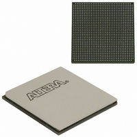
EP2SGX90EF1152C4N Altera, EP2SGX90EF1152C4N Datasheet - Page 5

EP2SGX90EF1152C4N
Manufacturer Part Number
EP2SGX90EF1152C4N
Description
IC STRATIX II GX 90K 1152-FBGA
Manufacturer
Altera
Series
Stratix® II GXr
Datasheet
1.EP2SGX30DF780C5.pdf
(316 pages)
Specifications of EP2SGX90EF1152C4N
Number Of Logic Elements/cells
90960
Number Of Labs/clbs
4548
Total Ram Bits
4520448
Number Of I /o
558
Voltage - Supply
1.15 V ~ 1.25 V
Mounting Type
Surface Mount
Operating Temperature
0°C ~ 70°C
Package / Case
1152-FBGA
Family Name
Stratix II GX
Number Of Logic Blocks/elements
90960
# I/os (max)
558
Frequency (max)
732.1MHz
Process Technology
SRAM
Operating Supply Voltage (typ)
1.2V
Logic Cells
90960
Ram Bits
4520448
Operating Supply Voltage (min)
1.15V
Operating Supply Voltage (max)
1.25V
Operating Temp Range
0C to 85C
Operating Temperature Classification
Commercial
Mounting
Surface Mount
Pin Count
1152
Package Type
FC-FBGA
For Use With
544-1725 - PCIE KIT W/S II GX EP2SGX90N544-1724 - SI KIT W/SII GX EP2SGX90N544-1702 - VIDEO KIT W/SII GX EP2SGX90N
Lead Free Status / RoHS Status
Lead free / RoHS Compliant
Number Of Gates
-
Lead Free Status / Rohs Status
Compliant
Other names
544-1767
EP2SGX90EF35C4NES
EP2SGX90EF35C4NES
Available stocks
Company
Part Number
Manufacturer
Quantity
Price
Company:
Part Number:
EP2SGX90EF1152C4N
Manufacturer:
ALTERA
Quantity:
648
- Current page: 5 of 316
- Download datasheet (2Mb)
Altera Corporation
October 2007
ALMs
Equivalent LEs
Transceiver
channels
Transceiver data rate
Source-synchronous
receive channels
Source-synchronous
transmit channels
M512 RAM blocks
(32 × 18 bits)
M4K RAM blocks
(128 × 36 bits)
M-RAM blocks
(4K × 144 bits)
Total RAM bits
Embedded
multipliers (18 × 18)
DSP blocks
PLLs
Maximum user I/O
pins
Table 1–1. Stratix II GX Device Features (Part 1 of 2)
Feature
f
(1)
EP2SGX30C/D
600 Mbps to
6.375 Gbps
C
1,369,728
4
13,552
33,880
202
144
361
31
29
64
16
Certain transceiver blocks can be bypassed. Refer to the
Architecture
more details.
Table 1–1
1
4
D
8
●
●
●
●
8B/10B encoder and decoder perform 8-bit to 10-bit encoding
and 10-bit to 8-bit decoding
Phase compensation FIFO buffer performs clock domain
translation between the transceiver block and the logic array
Receiver FIFO resynchronizes the received data with the local
reference clock
Channel aligner compliant with XAUI
lists the Stratix II GX device features.
600 Mbps to 6.375 Gbps
364
31
29
chapter in volume 1 of the Stratix II GX Device Handbook for
C
4
4
EP2SGX60C/D/E
2,544,192
24,176
60,440
364
31
29
329
255
144
D
8
4
36
2
534
12
42
42
E
8
Stratix II GX Device Handbook, Volume 1
558
12
47
45
E
EP2SGX90E/F
600 Mbps to
6.375 Gbps
4,520,448
36,384
90,960
488
408
192
48
4
8
650
16
59
59
F
Stratix II GX
EP2SGX130/G
600 Mbps to
6.375 Gbps
Introduction
6,747,840
132,540
53,016
699
609
252
734
20
73
71
63
G
6
8
1–3
Related parts for EP2SGX90EF1152C4N
Image
Part Number
Description
Manufacturer
Datasheet
Request
R

Part Number:
Description:
CYCLONE II STARTER KIT EP2C20N
Manufacturer:
Altera
Datasheet:

Part Number:
Description:
CPLD, EP610 Family, ECMOS Process, 300 Gates, 16 Macro Cells, 16 Reg., 16 User I/Os, 5V Supply, 35 Speed Grade, 24DIP
Manufacturer:
Altera Corporation
Datasheet:

Part Number:
Description:
CPLD, EP610 Family, ECMOS Process, 300 Gates, 16 Macro Cells, 16 Reg., 16 User I/Os, 5V Supply, 15 Speed Grade, 24DIP
Manufacturer:
Altera Corporation
Datasheet:

Part Number:
Description:
Manufacturer:
Altera Corporation
Datasheet:

Part Number:
Description:
CPLD, EP610 Family, ECMOS Process, 300 Gates, 16 Macro Cells, 16 Reg., 16 User I/Os, 5V Supply, 30 Speed Grade, 24DIP
Manufacturer:
Altera Corporation
Datasheet:

Part Number:
Description:
High-performance, low-power erasable programmable logic devices with 8 macrocells, 10ns
Manufacturer:
Altera Corporation
Datasheet:

Part Number:
Description:
High-performance, low-power erasable programmable logic devices with 8 macrocells, 7ns
Manufacturer:
Altera Corporation
Datasheet:

Part Number:
Description:
Classic EPLD
Manufacturer:
Altera Corporation
Datasheet:

Part Number:
Description:
High-performance, low-power erasable programmable logic devices with 8 macrocells, 10ns
Manufacturer:
Altera Corporation
Datasheet:

Part Number:
Description:
Manufacturer:
Altera Corporation
Datasheet:

Part Number:
Description:
Manufacturer:
Altera Corporation
Datasheet:

Part Number:
Description:
Manufacturer:
Altera Corporation
Datasheet:

Part Number:
Description:
CPLD, EP610 Family, ECMOS Process, 300 Gates, 16 Macro Cells, 16 Reg., 16 User I/Os, 5V Supply, 25 Speed Grade, 24DIP
Manufacturer:
Altera Corporation
Datasheet:


