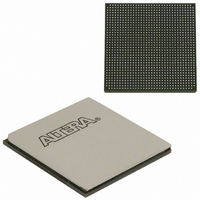
EP2SGX90EF1152C4N Altera, EP2SGX90EF1152C4N Datasheet - Page 52

EP2SGX90EF1152C4N
Manufacturer Part Number
EP2SGX90EF1152C4N
Description
IC STRATIX II GX 90K 1152-FBGA
Manufacturer
Altera
Series
Stratix® II GXr
Datasheet
1.EP2SGX30DF780C5.pdf
(316 pages)
Specifications of EP2SGX90EF1152C4N
Number Of Logic Elements/cells
90960
Number Of Labs/clbs
4548
Total Ram Bits
4520448
Number Of I /o
558
Voltage - Supply
1.15 V ~ 1.25 V
Mounting Type
Surface Mount
Operating Temperature
0°C ~ 70°C
Package / Case
1152-FBGA
Family Name
Stratix II GX
Number Of Logic Blocks/elements
90960
# I/os (max)
558
Frequency (max)
732.1MHz
Process Technology
SRAM
Operating Supply Voltage (typ)
1.2V
Logic Cells
90960
Ram Bits
4520448
Operating Supply Voltage (min)
1.15V
Operating Supply Voltage (max)
1.25V
Operating Temp Range
0C to 85C
Operating Temperature Classification
Commercial
Mounting
Surface Mount
Pin Count
1152
Package Type
FC-FBGA
For Use With
544-1725 - PCIE KIT W/S II GX EP2SGX90N544-1724 - SI KIT W/SII GX EP2SGX90N544-1702 - VIDEO KIT W/SII GX EP2SGX90N
Lead Free Status / RoHS Status
Lead free / RoHS Compliant
Number Of Gates
-
Lead Free Status / Rohs Status
Compliant
Other names
544-1767
EP2SGX90EF35C4NES
EP2SGX90EF35C4NES
Available stocks
Company
Part Number
Manufacturer
Quantity
Price
Company:
Part Number:
EP2SGX90EF1152C4N
Manufacturer:
ALTERA
Quantity:
648
- Current page: 52 of 316
- Download datasheet (2Mb)
Logic Array Blocks
Logic Array
Blocks
2–44
Stratix II GX Device Handbook, Volume 1
EP2SGX30
EP2SGX60
EP2SGX90
EP2SGX130
Table 2–17. Stratix II GX Device Resources
Device
Columns/Blocks
M512 RAM
6/202
7/329
8/488
9/699
Applications and Protocols Supported with Stratix II GX Devices
Each Stratix II GX transceiver block is designed to operate at any serial bit
rate from 600 Mbps to 6.375 Gbps per channel. The wide data rate range
allows Stratix II GX transceivers to support a wide variety of standards
and protocols, such as PCI Express, GIGE, SONET/SDH, SDI, OIF-CEI,
and XAUI. Stratix II GX devices are ideal for many high-speed
communication applications, such as high-speed backplanes,
chip-to-chip bridges, and high-speed serial communications links.
Example Applications Support for Stratix II GX
Stratix II GX devices can be used for many applications, including:
■
■
Each logic array block (LAB) consists of eight adaptive logic modules
(ALMs), carry chains, shared arithmetic chains, LAB control signals, local
interconnects, and register chain connection lines. The local interconnect
transfers signals between ALMs in the same LAB. Register chain
connections transfer the output of an ALM register to the adjacent ALM
register in a LAB. The Quartus II Compiler places associated logic in a
LAB or adjacent LABs, allowing the use of local, shared arithmetic chain,
and register chain connections for performance and area efficiency.
Table 2–17
Stratix II GX LAB structure.
Traffic management with various levels of quality of service (QoS)
and integrated serial backplane interconnect
Multi-port single-protocol switching (for example, PCI Express,
GIGE, XAUI switch, or SONET/SDH)
Columns/Blocks
M4K RAM
4/144
5/255
6/408
7/609
shows Stratix II GX device resources.
M-RAM
Blocks
1
2
4
6
Columns/Blocks
DSP Block
2/16
3/36
3/48
3/63
Figure 2–32
Columns
LAB
49
62
71
81
Altera Corporation
October 2007
shows the
LAB Rows
36
51
68
87
Related parts for EP2SGX90EF1152C4N
Image
Part Number
Description
Manufacturer
Datasheet
Request
R

Part Number:
Description:
CYCLONE II STARTER KIT EP2C20N
Manufacturer:
Altera
Datasheet:

Part Number:
Description:
CPLD, EP610 Family, ECMOS Process, 300 Gates, 16 Macro Cells, 16 Reg., 16 User I/Os, 5V Supply, 35 Speed Grade, 24DIP
Manufacturer:
Altera Corporation
Datasheet:

Part Number:
Description:
CPLD, EP610 Family, ECMOS Process, 300 Gates, 16 Macro Cells, 16 Reg., 16 User I/Os, 5V Supply, 15 Speed Grade, 24DIP
Manufacturer:
Altera Corporation
Datasheet:

Part Number:
Description:
Manufacturer:
Altera Corporation
Datasheet:

Part Number:
Description:
CPLD, EP610 Family, ECMOS Process, 300 Gates, 16 Macro Cells, 16 Reg., 16 User I/Os, 5V Supply, 30 Speed Grade, 24DIP
Manufacturer:
Altera Corporation
Datasheet:

Part Number:
Description:
High-performance, low-power erasable programmable logic devices with 8 macrocells, 10ns
Manufacturer:
Altera Corporation
Datasheet:

Part Number:
Description:
High-performance, low-power erasable programmable logic devices with 8 macrocells, 7ns
Manufacturer:
Altera Corporation
Datasheet:

Part Number:
Description:
Classic EPLD
Manufacturer:
Altera Corporation
Datasheet:

Part Number:
Description:
High-performance, low-power erasable programmable logic devices with 8 macrocells, 10ns
Manufacturer:
Altera Corporation
Datasheet:

Part Number:
Description:
Manufacturer:
Altera Corporation
Datasheet:

Part Number:
Description:
Manufacturer:
Altera Corporation
Datasheet:

Part Number:
Description:
Manufacturer:
Altera Corporation
Datasheet:

Part Number:
Description:
CPLD, EP610 Family, ECMOS Process, 300 Gates, 16 Macro Cells, 16 Reg., 16 User I/Os, 5V Supply, 25 Speed Grade, 24DIP
Manufacturer:
Altera Corporation
Datasheet:


