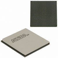
EP2SGX90EF1152C4N Altera, EP2SGX90EF1152C4N Datasheet - Page 305

EP2SGX90EF1152C4N
Manufacturer Part Number
EP2SGX90EF1152C4N
Description
IC STRATIX II GX 90K 1152-FBGA
Manufacturer
Altera
Series
Stratix® II GXr
Datasheet
1.EP2SGX30DF780C5.pdf
(316 pages)
Specifications of EP2SGX90EF1152C4N
Number Of Logic Elements/cells
90960
Number Of Labs/clbs
4548
Total Ram Bits
4520448
Number Of I /o
558
Voltage - Supply
1.15 V ~ 1.25 V
Mounting Type
Surface Mount
Operating Temperature
0°C ~ 70°C
Package / Case
1152-FBGA
Family Name
Stratix II GX
Number Of Logic Blocks/elements
90960
# I/os (max)
558
Frequency (max)
732.1MHz
Process Technology
SRAM
Operating Supply Voltage (typ)
1.2V
Logic Cells
90960
Ram Bits
4520448
Operating Supply Voltage (min)
1.15V
Operating Supply Voltage (max)
1.25V
Operating Temp Range
0C to 85C
Operating Temperature Classification
Commercial
Mounting
Surface Mount
Pin Count
1152
Package Type
FC-FBGA
For Use With
544-1725 - PCIE KIT W/S II GX EP2SGX90N544-1724 - SI KIT W/SII GX EP2SGX90N544-1702 - VIDEO KIT W/SII GX EP2SGX90N
Lead Free Status / RoHS Status
Lead free / RoHS Compliant
Number Of Gates
-
Lead Free Status / Rohs Status
Compliant
Other names
544-1767
EP2SGX90EF35C4NES
EP2SGX90EF35C4NES
Available stocks
Company
Part Number
Manufacturer
Quantity
Price
Company:
Part Number:
EP2SGX90EF1152C4N
Manufacturer:
ALTERA
Quantity:
648
- Current page: 305 of 316
- Download datasheet (2Mb)
Figure 4–14. Stratix II GX JTAG Waveforms.
Captured
Driven
Signal
Signal
to be
to be
TMS
TDO
TCK
TDI
t
JCH
Table 4–117
Stratix II GX devices.
t
t
t
t
t
t
t
t
t
t
t
t
t
t
t
JPZX
JSZX
JCP
JCH
JCL
JPSU
JPH
JPCO
JPZX
JPXZ
JSSU
JSH
JSCO
JSZX
JSXZ
Table 4–117. Stratix II GX JTAG Timing Parameters and Values
Symbol
t
JCP
t
JSSU
t
JCL
TCK clock period
TCK clock high time
TCK clock low time
JTAG port setup time
JTAG port hold time
JTAG port clock to output
JTAG port high impedance to valid output
JTAG port valid output to high impedance
Capture register setup time
Capture register hold time
Update register clock to output
Update register high impedance to valid output
Update register valid output to high impedance
shows the JTAG timing parameters and values for
t
JSH
t
t
JPCO
JSCO
t
JPSU
Parameter
t
t
JSXZ
JPH
t
JPXZ
Min Max Unit
30
12
12
4
5
4
5
12
12
12
9
9
9
ns
ns
ns
ns
ns
ns
ns
ns
ns
ns
ns
ns
ns
Related parts for EP2SGX90EF1152C4N
Image
Part Number
Description
Manufacturer
Datasheet
Request
R

Part Number:
Description:
CYCLONE II STARTER KIT EP2C20N
Manufacturer:
Altera
Datasheet:

Part Number:
Description:
CPLD, EP610 Family, ECMOS Process, 300 Gates, 16 Macro Cells, 16 Reg., 16 User I/Os, 5V Supply, 35 Speed Grade, 24DIP
Manufacturer:
Altera Corporation
Datasheet:

Part Number:
Description:
CPLD, EP610 Family, ECMOS Process, 300 Gates, 16 Macro Cells, 16 Reg., 16 User I/Os, 5V Supply, 15 Speed Grade, 24DIP
Manufacturer:
Altera Corporation
Datasheet:

Part Number:
Description:
Manufacturer:
Altera Corporation
Datasheet:

Part Number:
Description:
CPLD, EP610 Family, ECMOS Process, 300 Gates, 16 Macro Cells, 16 Reg., 16 User I/Os, 5V Supply, 30 Speed Grade, 24DIP
Manufacturer:
Altera Corporation
Datasheet:

Part Number:
Description:
High-performance, low-power erasable programmable logic devices with 8 macrocells, 10ns
Manufacturer:
Altera Corporation
Datasheet:

Part Number:
Description:
High-performance, low-power erasable programmable logic devices with 8 macrocells, 7ns
Manufacturer:
Altera Corporation
Datasheet:

Part Number:
Description:
Classic EPLD
Manufacturer:
Altera Corporation
Datasheet:

Part Number:
Description:
High-performance, low-power erasable programmable logic devices with 8 macrocells, 10ns
Manufacturer:
Altera Corporation
Datasheet:

Part Number:
Description:
Manufacturer:
Altera Corporation
Datasheet:

Part Number:
Description:
Manufacturer:
Altera Corporation
Datasheet:

Part Number:
Description:
Manufacturer:
Altera Corporation
Datasheet:

Part Number:
Description:
CPLD, EP610 Family, ECMOS Process, 300 Gates, 16 Macro Cells, 16 Reg., 16 User I/Os, 5V Supply, 25 Speed Grade, 24DIP
Manufacturer:
Altera Corporation
Datasheet:


