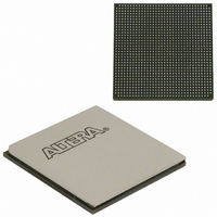
EP2SGX90EF1152C4N Altera, EP2SGX90EF1152C4N Datasheet - Page 78

EP2SGX90EF1152C4N
Manufacturer Part Number
EP2SGX90EF1152C4N
Description
IC STRATIX II GX 90K 1152-FBGA
Manufacturer
Altera
Series
Stratix® II GXr
Datasheet
1.EP2SGX30DF780C5.pdf
(316 pages)
Specifications of EP2SGX90EF1152C4N
Number Of Logic Elements/cells
90960
Number Of Labs/clbs
4548
Total Ram Bits
4520448
Number Of I /o
558
Voltage - Supply
1.15 V ~ 1.25 V
Mounting Type
Surface Mount
Operating Temperature
0°C ~ 70°C
Package / Case
1152-FBGA
Family Name
Stratix II GX
Number Of Logic Blocks/elements
90960
# I/os (max)
558
Frequency (max)
732.1MHz
Process Technology
SRAM
Operating Supply Voltage (typ)
1.2V
Logic Cells
90960
Ram Bits
4520448
Operating Supply Voltage (min)
1.15V
Operating Supply Voltage (max)
1.25V
Operating Temp Range
0C to 85C
Operating Temperature Classification
Commercial
Mounting
Surface Mount
Pin Count
1152
Package Type
FC-FBGA
For Use With
544-1725 - PCIE KIT W/S II GX EP2SGX90N544-1724 - SI KIT W/SII GX EP2SGX90N544-1702 - VIDEO KIT W/SII GX EP2SGX90N
Lead Free Status / RoHS Status
Lead free / RoHS Compliant
Number Of Gates
-
Lead Free Status / Rohs Status
Compliant
Other names
544-1767
EP2SGX90EF35C4NES
EP2SGX90EF35C4NES
Available stocks
Company
Part Number
Manufacturer
Quantity
Price
Company:
Part Number:
EP2SGX90EF1152C4N
Manufacturer:
ALTERA
Quantity:
648
- Current page: 78 of 316
- Download datasheet (2Mb)
TriMatrix Memory
2–70
Stratix II GX Device Handbook, Volume 1
Note to
(1)
Simple dual-port memory
mixed width support
True dual-port memory
mixed width support
Power-up conditions
Register clears
Mixed-port read-during-write Unknown output/old data Unknown output/old data
Configurations
Table 2–19. TriMatrix Memory Features (Part 2 of 2)
Violating the setup or hold time on the memory block address registers could corrupt memory contents. This
applies to both read and write operations.
Memory Feature
Table
2–19:
TriMatrix memory provides three different memory sizes for efficient
application support. The Quartus II software automatically partitions the
user-defined memory into the embedded memory blocks using the most
efficient size combinations. You can also manually assign the memory to
a specific block size or a mixture of block sizes.
M512 RAM Block
The M512 RAM block is a simple dual-port memory block and is useful
for implementing small FIFO buffers, DSP, and clock domain transfer
applications. Each block contains 576 RAM bits (including parity bits).
M512 RAM blocks can be configured in the following modes:
■
■
■
■
■
When configured as RAM or ROM, you can use an initialization file to
pre-load the memory contents.
M512 RAM Block
Simple dual-port RAM
Single-port RAM
FIFO
ROM
Shift register
Output registers
Outputs cleared
(32 × 18 Bits)
512 × 1
256 × 2
128 × 4
32 × 16
32 × 18
64 × 8
64 × 9
v
M4K RAM Block
Output registers
Outputs cleared
(128 × 36 Bits)
256 × 16
256 × 18
128 × 32
128 × 36
512 × 8
512 × 9
4K × 1
2K × 2
1K × 4
v
v
Outputs unknown
Unknown output
Output registers
(4K × 144 Bits)
M-RAM Block
Altera Corporation
32K × 16
32K × 18
16K × 32
16K × 36
4K × 128
4K × 144
64K × 8
64K × 9
8K × 64
8K × 72
v
v
October 2007
Related parts for EP2SGX90EF1152C4N
Image
Part Number
Description
Manufacturer
Datasheet
Request
R

Part Number:
Description:
CYCLONE II STARTER KIT EP2C20N
Manufacturer:
Altera
Datasheet:

Part Number:
Description:
CPLD, EP610 Family, ECMOS Process, 300 Gates, 16 Macro Cells, 16 Reg., 16 User I/Os, 5V Supply, 35 Speed Grade, 24DIP
Manufacturer:
Altera Corporation
Datasheet:

Part Number:
Description:
CPLD, EP610 Family, ECMOS Process, 300 Gates, 16 Macro Cells, 16 Reg., 16 User I/Os, 5V Supply, 15 Speed Grade, 24DIP
Manufacturer:
Altera Corporation
Datasheet:

Part Number:
Description:
Manufacturer:
Altera Corporation
Datasheet:

Part Number:
Description:
CPLD, EP610 Family, ECMOS Process, 300 Gates, 16 Macro Cells, 16 Reg., 16 User I/Os, 5V Supply, 30 Speed Grade, 24DIP
Manufacturer:
Altera Corporation
Datasheet:

Part Number:
Description:
High-performance, low-power erasable programmable logic devices with 8 macrocells, 10ns
Manufacturer:
Altera Corporation
Datasheet:

Part Number:
Description:
High-performance, low-power erasable programmable logic devices with 8 macrocells, 7ns
Manufacturer:
Altera Corporation
Datasheet:

Part Number:
Description:
Classic EPLD
Manufacturer:
Altera Corporation
Datasheet:

Part Number:
Description:
High-performance, low-power erasable programmable logic devices with 8 macrocells, 10ns
Manufacturer:
Altera Corporation
Datasheet:

Part Number:
Description:
Manufacturer:
Altera Corporation
Datasheet:

Part Number:
Description:
Manufacturer:
Altera Corporation
Datasheet:

Part Number:
Description:
Manufacturer:
Altera Corporation
Datasheet:

Part Number:
Description:
CPLD, EP610 Family, ECMOS Process, 300 Gates, 16 Macro Cells, 16 Reg., 16 User I/Os, 5V Supply, 25 Speed Grade, 24DIP
Manufacturer:
Altera Corporation
Datasheet:


