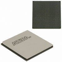
EP2SGX90EF1152C4N Altera, EP2SGX90EF1152C4N Datasheet - Page 159

EP2SGX90EF1152C4N
Manufacturer Part Number
EP2SGX90EF1152C4N
Description
IC STRATIX II GX 90K 1152-FBGA
Manufacturer
Altera
Series
Stratix® II GXr
Datasheet
1.EP2SGX30DF780C5.pdf
(316 pages)
Specifications of EP2SGX90EF1152C4N
Number Of Logic Elements/cells
90960
Number Of Labs/clbs
4548
Total Ram Bits
4520448
Number Of I /o
558
Voltage - Supply
1.15 V ~ 1.25 V
Mounting Type
Surface Mount
Operating Temperature
0°C ~ 70°C
Package / Case
1152-FBGA
Family Name
Stratix II GX
Number Of Logic Blocks/elements
90960
# I/os (max)
558
Frequency (max)
732.1MHz
Process Technology
SRAM
Operating Supply Voltage (typ)
1.2V
Logic Cells
90960
Ram Bits
4520448
Operating Supply Voltage (min)
1.15V
Operating Supply Voltage (max)
1.25V
Operating Temp Range
0C to 85C
Operating Temperature Classification
Commercial
Mounting
Surface Mount
Pin Count
1152
Package Type
FC-FBGA
For Use With
544-1725 - PCIE KIT W/S II GX EP2SGX90N544-1724 - SI KIT W/SII GX EP2SGX90N544-1702 - VIDEO KIT W/SII GX EP2SGX90N
Lead Free Status / RoHS Status
Lead free / RoHS Compliant
Number Of Gates
-
Lead Free Status / Rohs Status
Compliant
Other names
544-1767
EP2SGX90EF35C4NES
EP2SGX90EF35C4NES
Available stocks
Company
Part Number
Manufacturer
Quantity
Price
Company:
Part Number:
EP2SGX90EF1152C4N
Manufacturer:
ALTERA
Quantity:
648
- Current page: 159 of 316
- Download datasheet (2Mb)
SignalTap II
Embedded Logic
Analyzer
Configuration
Altera Corporation
October 2007
EP2SGX30
EP2SGX60
EP2SGX90
EP2SGX130
Table 3–3. 32-Bit Stratix II GX Device IDCODE
Device
Version (4 Bits)
0000
0000
0000
0000
The Stratix II GX device instruction register length is 10 bits and the
USERCODE
scan register length and device IDCODE information for Stratix II GX
devices.
Stratix II GX devices feature the SignalTap II embedded logic analyzer,
which monitors design operation over a period of time through the IEEE
Std. 1149.1 (JTAG) circuitry. You can analyze internal logic at speed
without bringing internal signals to the I/O pins. This feature is
particularly important for advanced packages, such as FineLine BGA
packages, because it can be difficult to add a connection to a pin during
the debugging process after a board is designed and manufactured.
The logic, circuitry, and interconnects in the Stratix II GX architecture are
configured with CMOS SRAM elements. Altera
reconfigurable and every device is tested with a high coverage
production test program so you do not have to perform fault testing and
can instead focus on simulation and design verification.
Stratix II GX devices are configured at system power-up with data stored
in an Altera configuration device or provided by an external controller
(for example, a MAX
Stratix II GX devices using the fast passive parallel (FPP), active serial
Table 3–2. Stratix II GX Boundary-Scan Register Length
register length is 32 bits.
0010 0000 1110 0001
0010 0000 1110 0010
0010 0000 1110 0011
0010 0000 1110 0100
EP2SGX130
Part Number (16 Bits)
EP2SGX30
EP2SGX60
EP2SGX90
Device
®
II device or microprocessor). You can configure
IDCODE (32 Bits)
Stratix II GX Device Handbook, Volume 1
Tables 3–2
Manufacturer Identity
000 0110 1110
000 0110 1110
000 0110 1110
000 0110 1110
Boundary-Scan Register Length
(11 Bits)
and
®
3–3
FPGAs are
Configuration & Testing
1,320
1,506
2,016
2,454
show the boundary-
LSB (1 Bit)
1
1
1
1
3–3
Related parts for EP2SGX90EF1152C4N
Image
Part Number
Description
Manufacturer
Datasheet
Request
R

Part Number:
Description:
CYCLONE II STARTER KIT EP2C20N
Manufacturer:
Altera
Datasheet:

Part Number:
Description:
CPLD, EP610 Family, ECMOS Process, 300 Gates, 16 Macro Cells, 16 Reg., 16 User I/Os, 5V Supply, 35 Speed Grade, 24DIP
Manufacturer:
Altera Corporation
Datasheet:

Part Number:
Description:
CPLD, EP610 Family, ECMOS Process, 300 Gates, 16 Macro Cells, 16 Reg., 16 User I/Os, 5V Supply, 15 Speed Grade, 24DIP
Manufacturer:
Altera Corporation
Datasheet:

Part Number:
Description:
Manufacturer:
Altera Corporation
Datasheet:

Part Number:
Description:
CPLD, EP610 Family, ECMOS Process, 300 Gates, 16 Macro Cells, 16 Reg., 16 User I/Os, 5V Supply, 30 Speed Grade, 24DIP
Manufacturer:
Altera Corporation
Datasheet:

Part Number:
Description:
High-performance, low-power erasable programmable logic devices with 8 macrocells, 10ns
Manufacturer:
Altera Corporation
Datasheet:

Part Number:
Description:
High-performance, low-power erasable programmable logic devices with 8 macrocells, 7ns
Manufacturer:
Altera Corporation
Datasheet:

Part Number:
Description:
Classic EPLD
Manufacturer:
Altera Corporation
Datasheet:

Part Number:
Description:
High-performance, low-power erasable programmable logic devices with 8 macrocells, 10ns
Manufacturer:
Altera Corporation
Datasheet:

Part Number:
Description:
Manufacturer:
Altera Corporation
Datasheet:

Part Number:
Description:
Manufacturer:
Altera Corporation
Datasheet:

Part Number:
Description:
Manufacturer:
Altera Corporation
Datasheet:

Part Number:
Description:
CPLD, EP610 Family, ECMOS Process, 300 Gates, 16 Macro Cells, 16 Reg., 16 User I/Os, 5V Supply, 25 Speed Grade, 24DIP
Manufacturer:
Altera Corporation
Datasheet:


