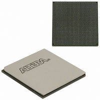
EP2SGX90EF1152C4N Altera, EP2SGX90EF1152C4N Datasheet - Page 302

EP2SGX90EF1152C4N
Manufacturer Part Number
EP2SGX90EF1152C4N
Description
IC STRATIX II GX 90K 1152-FBGA
Manufacturer
Altera
Series
Stratix® II GXr
Datasheet
1.EP2SGX30DF780C5.pdf
(316 pages)
Specifications of EP2SGX90EF1152C4N
Number Of Logic Elements/cells
90960
Number Of Labs/clbs
4548
Total Ram Bits
4520448
Number Of I /o
558
Voltage - Supply
1.15 V ~ 1.25 V
Mounting Type
Surface Mount
Operating Temperature
0°C ~ 70°C
Package / Case
1152-FBGA
Family Name
Stratix II GX
Number Of Logic Blocks/elements
90960
# I/os (max)
558
Frequency (max)
732.1MHz
Process Technology
SRAM
Operating Supply Voltage (typ)
1.2V
Logic Cells
90960
Ram Bits
4520448
Operating Supply Voltage (min)
1.15V
Operating Supply Voltage (max)
1.25V
Operating Temp Range
0C to 85C
Operating Temperature Classification
Commercial
Mounting
Surface Mount
Pin Count
1152
Package Type
FC-FBGA
For Use With
544-1725 - PCIE KIT W/S II GX EP2SGX90N544-1724 - SI KIT W/SII GX EP2SGX90N544-1702 - VIDEO KIT W/SII GX EP2SGX90N
Lead Free Status / RoHS Status
Lead free / RoHS Compliant
Number Of Gates
-
Lead Free Status / Rohs Status
Compliant
Other names
544-1767
EP2SGX90EF35C4NES
EP2SGX90EF35C4NES
Available stocks
Company
Part Number
Manufacturer
Quantity
Price
Company:
Part Number:
EP2SGX90EF1152C4N
Manufacturer:
ALTERA
Quantity:
648
- Current page: 302 of 316
- Download datasheet (2Mb)
External
Memory
Interface
Specifications
(1)
f
f
f
t
f
t
t
t
t
VCO
OUT
OUT_EXT
CONFIGPLL
CLBW
LOCK
PLL_PSERR
ARESET
ARESET_RECONFIG
Table 4–111. Fast PLL Specifications (Part 2 of 2)
This is limited by the I/O f
Name
Upper VCO frequency range for –3 and –4
speed grades
Upper VCO frequency range for –5 speed
grades
Lower VCO frequency range for –3 and –4
speed grades
Lower VCO frequency range for –5 speed
grades
PLL output frequency to
PLL output frequency to LVDS or DPA clock
PLL clock output frequency to regular I/O
Time required to reconfigure scan chains for
fast PLLs
PLL closed-loop bandwidth
Time required for the PLL to lock from the
time it is enabled or the end of the device
configuration
Accuracy of PLL phase shift
Minimum pulse width on
Minimum pulse width on the
when using PLL reconfiguration. Reset the
PLL after
Tables 4–112
the dedicated circuitry used for interfacing with external memory
devices.
MAX
Table 4–112. DLL Frequency Range Specifications (Part 1 of 2)
scandone
Frequency Mode
. See
Description
Tables 4–91
0
1
2
goes high.
through
GCLK
areset
through
areset
or
200 to 310 (–4 and –5 speed grade)
4–116
RCLK
signal.
200 to 350 (–3 speed grade)
4–95
Frequency Range (MHz)
signal
contain Stratix II GX device specifications for
for the maximum.
100 to 175
150 to 230
4.6875
4.6875
1.16
Min
300
300
150
150
150
500
10
75/f
0.03
SCANCLK
Typ
5
1,040
1,040
Max
±30
840
520
420
550
(1)
Resolution
28
(Degrees)
1
22.5
30
30
30
MHz
MHz
MHz
MHz
MHz
MHz
MHz
MHz
Unit
ms
ns
ps
ns
ns
Related parts for EP2SGX90EF1152C4N
Image
Part Number
Description
Manufacturer
Datasheet
Request
R

Part Number:
Description:
CYCLONE II STARTER KIT EP2C20N
Manufacturer:
Altera
Datasheet:

Part Number:
Description:
CPLD, EP610 Family, ECMOS Process, 300 Gates, 16 Macro Cells, 16 Reg., 16 User I/Os, 5V Supply, 35 Speed Grade, 24DIP
Manufacturer:
Altera Corporation
Datasheet:

Part Number:
Description:
CPLD, EP610 Family, ECMOS Process, 300 Gates, 16 Macro Cells, 16 Reg., 16 User I/Os, 5V Supply, 15 Speed Grade, 24DIP
Manufacturer:
Altera Corporation
Datasheet:

Part Number:
Description:
Manufacturer:
Altera Corporation
Datasheet:

Part Number:
Description:
CPLD, EP610 Family, ECMOS Process, 300 Gates, 16 Macro Cells, 16 Reg., 16 User I/Os, 5V Supply, 30 Speed Grade, 24DIP
Manufacturer:
Altera Corporation
Datasheet:

Part Number:
Description:
High-performance, low-power erasable programmable logic devices with 8 macrocells, 10ns
Manufacturer:
Altera Corporation
Datasheet:

Part Number:
Description:
High-performance, low-power erasable programmable logic devices with 8 macrocells, 7ns
Manufacturer:
Altera Corporation
Datasheet:

Part Number:
Description:
Classic EPLD
Manufacturer:
Altera Corporation
Datasheet:

Part Number:
Description:
High-performance, low-power erasable programmable logic devices with 8 macrocells, 10ns
Manufacturer:
Altera Corporation
Datasheet:

Part Number:
Description:
Manufacturer:
Altera Corporation
Datasheet:

Part Number:
Description:
Manufacturer:
Altera Corporation
Datasheet:

Part Number:
Description:
Manufacturer:
Altera Corporation
Datasheet:

Part Number:
Description:
CPLD, EP610 Family, ECMOS Process, 300 Gates, 16 Macro Cells, 16 Reg., 16 User I/Os, 5V Supply, 25 Speed Grade, 24DIP
Manufacturer:
Altera Corporation
Datasheet:


