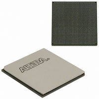
EP2SGX90EF1152C4N Altera, EP2SGX90EF1152C4N Datasheet - Page 31

EP2SGX90EF1152C4N
Manufacturer Part Number
EP2SGX90EF1152C4N
Description
IC STRATIX II GX 90K 1152-FBGA
Manufacturer
Altera
Series
Stratix® II GXr
Datasheet
1.EP2SGX30DF780C5.pdf
(316 pages)
Specifications of EP2SGX90EF1152C4N
Number Of Logic Elements/cells
90960
Number Of Labs/clbs
4548
Total Ram Bits
4520448
Number Of I /o
558
Voltage - Supply
1.15 V ~ 1.25 V
Mounting Type
Surface Mount
Operating Temperature
0°C ~ 70°C
Package / Case
1152-FBGA
Family Name
Stratix II GX
Number Of Logic Blocks/elements
90960
# I/os (max)
558
Frequency (max)
732.1MHz
Process Technology
SRAM
Operating Supply Voltage (typ)
1.2V
Logic Cells
90960
Ram Bits
4520448
Operating Supply Voltage (min)
1.15V
Operating Supply Voltage (max)
1.25V
Operating Temp Range
0C to 85C
Operating Temperature Classification
Commercial
Mounting
Surface Mount
Pin Count
1152
Package Type
FC-FBGA
For Use With
544-1725 - PCIE KIT W/S II GX EP2SGX90N544-1724 - SI KIT W/SII GX EP2SGX90N544-1702 - VIDEO KIT W/SII GX EP2SGX90N
Lead Free Status / RoHS Status
Lead free / RoHS Compliant
Number Of Gates
-
Lead Free Status / Rohs Status
Compliant
Other names
544-1767
EP2SGX90EF35C4NES
EP2SGX90EF35C4NES
Available stocks
Company
Part Number
Manufacturer
Quantity
Price
Company:
Part Number:
EP2SGX90EF1152C4N
Manufacturer:
ALTERA
Quantity:
648
- Current page: 31 of 316
- Download datasheet (2Mb)
Altera Corporation
October 2007
Programmable Run Length Violation
The word aligner supports a programmable run length violation counter.
Whenever the number of the continuous ‘0’ (or ‘1’) exceeds a user
programmable value, the rx_rlv signal goes high for a minimum pulse
width of two recovered clock cycles. The maximum run values supported
are shown in
Running Disparity Check
The running disparity error rx_disperr and running disparity value
rx_runningdisp are sent along with aligned data from the 8B/10B
decoder to the FPGA. You can ignore or act on the reported running
disparity value and running disparity error signals.
Bit-Slip Mode
The word aligner can operate in either pattern detection mode or in
bit-slip mode.
The bit-slip mode provides the option to manually shift the word
boundary through the FPGA. This feature is useful for:
■
■
■
This feature can be applied at 10-bit and 16-bit data widths.
The word aligner outputs a word boundary as it is received from the
analog receiver after reset. You can examine the word and search its
boundary in the FPGA. To do so, assert the rx_bitslip signal. The
rx_bitslip signal should be toggled and held constant for at least two
FPGA clock cycles.
For every rising edge of the rx_bitslip signal, the current word
boundary is slipped by one bit. Every time a bit is slipped, the bit received
earliest is lost. If bit slipping shifts a complete round of bus width, the
word boundary is back to the original boundary.
Single-Width
Double-Width
Table 2–7. Maximum Run Length (UI)
Longer synchronization patterns than the pattern detector can
accommodate
Scrambled data stream
Input stream consisting of over-sampled data
Mode
Table
8 Bit
2–7.
128
—
10 Bit
Stratix II GX Device Handbook, Volume 1
160
—
PMA Serialization
16 Bit
512
Stratix II GX Architecture
—
20 Bit
640
—
2–23
Related parts for EP2SGX90EF1152C4N
Image
Part Number
Description
Manufacturer
Datasheet
Request
R

Part Number:
Description:
CYCLONE II STARTER KIT EP2C20N
Manufacturer:
Altera
Datasheet:

Part Number:
Description:
CPLD, EP610 Family, ECMOS Process, 300 Gates, 16 Macro Cells, 16 Reg., 16 User I/Os, 5V Supply, 35 Speed Grade, 24DIP
Manufacturer:
Altera Corporation
Datasheet:

Part Number:
Description:
CPLD, EP610 Family, ECMOS Process, 300 Gates, 16 Macro Cells, 16 Reg., 16 User I/Os, 5V Supply, 15 Speed Grade, 24DIP
Manufacturer:
Altera Corporation
Datasheet:

Part Number:
Description:
Manufacturer:
Altera Corporation
Datasheet:

Part Number:
Description:
CPLD, EP610 Family, ECMOS Process, 300 Gates, 16 Macro Cells, 16 Reg., 16 User I/Os, 5V Supply, 30 Speed Grade, 24DIP
Manufacturer:
Altera Corporation
Datasheet:

Part Number:
Description:
High-performance, low-power erasable programmable logic devices with 8 macrocells, 10ns
Manufacturer:
Altera Corporation
Datasheet:

Part Number:
Description:
High-performance, low-power erasable programmable logic devices with 8 macrocells, 7ns
Manufacturer:
Altera Corporation
Datasheet:

Part Number:
Description:
Classic EPLD
Manufacturer:
Altera Corporation
Datasheet:

Part Number:
Description:
High-performance, low-power erasable programmable logic devices with 8 macrocells, 10ns
Manufacturer:
Altera Corporation
Datasheet:

Part Number:
Description:
Manufacturer:
Altera Corporation
Datasheet:

Part Number:
Description:
Manufacturer:
Altera Corporation
Datasheet:

Part Number:
Description:
Manufacturer:
Altera Corporation
Datasheet:

Part Number:
Description:
CPLD, EP610 Family, ECMOS Process, 300 Gates, 16 Macro Cells, 16 Reg., 16 User I/Os, 5V Supply, 25 Speed Grade, 24DIP
Manufacturer:
Altera Corporation
Datasheet:


