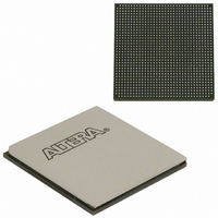
EP2SGX90EF1152C4N Altera, EP2SGX90EF1152C4N Datasheet - Page 146

EP2SGX90EF1152C4N
Manufacturer Part Number
EP2SGX90EF1152C4N
Description
IC STRATIX II GX 90K 1152-FBGA
Manufacturer
Altera
Series
Stratix® II GXr
Datasheet
1.EP2SGX30DF780C5.pdf
(316 pages)
Specifications of EP2SGX90EF1152C4N
Number Of Logic Elements/cells
90960
Number Of Labs/clbs
4548
Total Ram Bits
4520448
Number Of I /o
558
Voltage - Supply
1.15 V ~ 1.25 V
Mounting Type
Surface Mount
Operating Temperature
0°C ~ 70°C
Package / Case
1152-FBGA
Family Name
Stratix II GX
Number Of Logic Blocks/elements
90960
# I/os (max)
558
Frequency (max)
732.1MHz
Process Technology
SRAM
Operating Supply Voltage (typ)
1.2V
Logic Cells
90960
Ram Bits
4520448
Operating Supply Voltage (min)
1.15V
Operating Supply Voltage (max)
1.25V
Operating Temp Range
0C to 85C
Operating Temperature Classification
Commercial
Mounting
Surface Mount
Pin Count
1152
Package Type
FC-FBGA
For Use With
544-1725 - PCIE KIT W/S II GX EP2SGX90N544-1724 - SI KIT W/SII GX EP2SGX90N544-1702 - VIDEO KIT W/SII GX EP2SGX90N
Lead Free Status / RoHS Status
Lead free / RoHS Compliant
Number Of Gates
-
Lead Free Status / Rohs Status
Compliant
Other names
544-1767
EP2SGX90EF35C4NES
EP2SGX90EF35C4NES
Available stocks
Company
Part Number
Manufacturer
Quantity
Price
Company:
Part Number:
EP2SGX90EF1152C4N
Manufacturer:
ALTERA
Quantity:
648
- Current page: 146 of 316
- Download datasheet (2Mb)
High-Speed Differential I/O with DPA Support
2–138
Stratix II GX Device Handbook, Volume 1
Note to
(1)
1508-pin FineLine BGA
Table 2–41. EP2SGX130 Device Differential Channels
The total number of receiver channels includes the four non-dedicated clock channels that can be optionally used
as data channels.
Package
Tables 2–38
through 2–41:
Transmitter/Receiver
Therefore, the total number of channels is not the addition of the number
of channels accessible by PLLs 1 and 2 with the number of channels
accessible by PLLs 7 and 8.
Dedicated Circuitry with DPA Support
Stratix II GX devices support source-synchronous interfacing with LVDS
signaling at up to 1 Gbps. Stratix II GX devices can transmit or receive
serial channels along with a low-speed or high-speed clock.
The receiving device PLL multiplies the clock by an integer factor W = 1
through 32. The SERDES factor J determines the parallel data width to
deserialize from receivers or to serialize for transmitters. The SERDES
factor J can be set to 4, 5, 6, 7, 8, 9, or 10 and does not have to equal the PLL
clock-multiplication W value. A design using the dynamic phase aligner
also supports all of these J factor values. For a J factor of 1, the
Stratix II GX device bypasses the SERDES block. For a J factor of 2, the
Stratix II GX device bypasses the SERDES block, and the DDR input and
output registers are used in the IOE.
of the Stratix II GX transmitter channel.
Transmitter
Receiver
Channels
Total
71
73
Note (1)
Center Fast PLLs
PLL1
37
37
Figure 2–88
PLL2
41
41
shows the block diagram
PLL7
Corner Fast PLLs
37
37
Altera Corporation
October 2007
PLL8
41
41
Related parts for EP2SGX90EF1152C4N
Image
Part Number
Description
Manufacturer
Datasheet
Request
R

Part Number:
Description:
CYCLONE II STARTER KIT EP2C20N
Manufacturer:
Altera
Datasheet:

Part Number:
Description:
CPLD, EP610 Family, ECMOS Process, 300 Gates, 16 Macro Cells, 16 Reg., 16 User I/Os, 5V Supply, 35 Speed Grade, 24DIP
Manufacturer:
Altera Corporation
Datasheet:

Part Number:
Description:
CPLD, EP610 Family, ECMOS Process, 300 Gates, 16 Macro Cells, 16 Reg., 16 User I/Os, 5V Supply, 15 Speed Grade, 24DIP
Manufacturer:
Altera Corporation
Datasheet:

Part Number:
Description:
Manufacturer:
Altera Corporation
Datasheet:

Part Number:
Description:
CPLD, EP610 Family, ECMOS Process, 300 Gates, 16 Macro Cells, 16 Reg., 16 User I/Os, 5V Supply, 30 Speed Grade, 24DIP
Manufacturer:
Altera Corporation
Datasheet:

Part Number:
Description:
High-performance, low-power erasable programmable logic devices with 8 macrocells, 10ns
Manufacturer:
Altera Corporation
Datasheet:

Part Number:
Description:
High-performance, low-power erasable programmable logic devices with 8 macrocells, 7ns
Manufacturer:
Altera Corporation
Datasheet:

Part Number:
Description:
Classic EPLD
Manufacturer:
Altera Corporation
Datasheet:

Part Number:
Description:
High-performance, low-power erasable programmable logic devices with 8 macrocells, 10ns
Manufacturer:
Altera Corporation
Datasheet:

Part Number:
Description:
Manufacturer:
Altera Corporation
Datasheet:

Part Number:
Description:
Manufacturer:
Altera Corporation
Datasheet:

Part Number:
Description:
Manufacturer:
Altera Corporation
Datasheet:

Part Number:
Description:
CPLD, EP610 Family, ECMOS Process, 300 Gates, 16 Macro Cells, 16 Reg., 16 User I/Os, 5V Supply, 25 Speed Grade, 24DIP
Manufacturer:
Altera Corporation
Datasheet:


