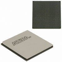
EP2SGX90EF1152C4N Altera, EP2SGX90EF1152C4N Datasheet - Page 218

EP2SGX90EF1152C4N
Manufacturer Part Number
EP2SGX90EF1152C4N
Description
IC STRATIX II GX 90K 1152-FBGA
Manufacturer
Altera
Series
Stratix® II GXr
Datasheet
1.EP2SGX30DF780C5.pdf
(316 pages)
Specifications of EP2SGX90EF1152C4N
Number Of Logic Elements/cells
90960
Number Of Labs/clbs
4548
Total Ram Bits
4520448
Number Of I /o
558
Voltage - Supply
1.15 V ~ 1.25 V
Mounting Type
Surface Mount
Operating Temperature
0°C ~ 70°C
Package / Case
1152-FBGA
Family Name
Stratix II GX
Number Of Logic Blocks/elements
90960
# I/os (max)
558
Frequency (max)
732.1MHz
Process Technology
SRAM
Operating Supply Voltage (typ)
1.2V
Logic Cells
90960
Ram Bits
4520448
Operating Supply Voltage (min)
1.15V
Operating Supply Voltage (max)
1.25V
Operating Temp Range
0C to 85C
Operating Temperature Classification
Commercial
Mounting
Surface Mount
Pin Count
1152
Package Type
FC-FBGA
For Use With
544-1725 - PCIE KIT W/S II GX EP2SGX90N544-1724 - SI KIT W/SII GX EP2SGX90N544-1702 - VIDEO KIT W/SII GX EP2SGX90N
Lead Free Status / RoHS Status
Lead free / RoHS Compliant
Number Of Gates
-
Lead Free Status / Rohs Status
Compliant
Other names
544-1767
EP2SGX90EF35C4NES
EP2SGX90EF35C4NES
Available stocks
Company
Part Number
Manufacturer
Quantity
Price
Company:
Part Number:
EP2SGX90EF1152C4N
Manufacturer:
ALTERA
Quantity:
648
- Current page: 218 of 316
- Download datasheet (2Mb)
Operating Conditions
4–48
Stratix II GX Device Handbook, Volume 1
Note to
(1)
Reference Clock
3.3-V PCML
1.5-V PCML
1.2-V PCML
V
V
R
Receiver
3.3-V PCML
1.5-V PCML
1.2-V PCML
V
V
R
Transmitter
1.5-V PCML
1.2-V PCML
V
V
V
R
Table 4–31. PCML Specifications
ID
ICM
ID
ICM
CCH
OD
OCM
Symbol
Stratix II GX devices support PCML input and output on GXB banks 13, 14, 15, 16, and 17. This table references
Stratix II GX PCML specifications that are located in other sections of the Stratix II GX Device Handbook.
Table
4–31:
Reference clock supported
PCML standards
Peak-to-peak differential input
voltage
Input common mode voltage
On-chip termination resistors
Receiver supported PCML
standards
Peak-to-peak differential input
voltage
Input common mode voltage
On-chip termination resistors
Transmitter supported PCML
standards
Output buffer supply voltage
Peak-to-peak differential output
voltage
Output common mode voltage
On-chip termination resistors
Parameter
Note (1)
The specifications are located in the Reference Clock section
of
The specifications listed in
input standards.
The specifications are located in the Receiver section of
Table 4–6 on page
The specifications listed in
input standards.
The specifications are located in
The specifications are located in
4–11, and 4–12.
The specifications listed in these tables are applicable to
PCML output standards.
The specifications are located in the Transmitter section of
Table 4–6 on page
The specifications listed in
output standards.
Table 4–6 on page
4–4.
4–4.
4–4.
References
Table 4–6
Table 4–6
Table 4–6
Tables
Table 4–5 on page
are applicable to PCML
are applicable to PCML
are applicable to PCML
4–7, 4–8, 4–9, 4–10,
Altera Corporation
June 2009
4–4.
Related parts for EP2SGX90EF1152C4N
Image
Part Number
Description
Manufacturer
Datasheet
Request
R

Part Number:
Description:
CYCLONE II STARTER KIT EP2C20N
Manufacturer:
Altera
Datasheet:

Part Number:
Description:
CPLD, EP610 Family, ECMOS Process, 300 Gates, 16 Macro Cells, 16 Reg., 16 User I/Os, 5V Supply, 35 Speed Grade, 24DIP
Manufacturer:
Altera Corporation
Datasheet:

Part Number:
Description:
CPLD, EP610 Family, ECMOS Process, 300 Gates, 16 Macro Cells, 16 Reg., 16 User I/Os, 5V Supply, 15 Speed Grade, 24DIP
Manufacturer:
Altera Corporation
Datasheet:

Part Number:
Description:
Manufacturer:
Altera Corporation
Datasheet:

Part Number:
Description:
CPLD, EP610 Family, ECMOS Process, 300 Gates, 16 Macro Cells, 16 Reg., 16 User I/Os, 5V Supply, 30 Speed Grade, 24DIP
Manufacturer:
Altera Corporation
Datasheet:

Part Number:
Description:
High-performance, low-power erasable programmable logic devices with 8 macrocells, 10ns
Manufacturer:
Altera Corporation
Datasheet:

Part Number:
Description:
High-performance, low-power erasable programmable logic devices with 8 macrocells, 7ns
Manufacturer:
Altera Corporation
Datasheet:

Part Number:
Description:
Classic EPLD
Manufacturer:
Altera Corporation
Datasheet:

Part Number:
Description:
High-performance, low-power erasable programmable logic devices with 8 macrocells, 10ns
Manufacturer:
Altera Corporation
Datasheet:

Part Number:
Description:
Manufacturer:
Altera Corporation
Datasheet:

Part Number:
Description:
Manufacturer:
Altera Corporation
Datasheet:

Part Number:
Description:
Manufacturer:
Altera Corporation
Datasheet:

Part Number:
Description:
CPLD, EP610 Family, ECMOS Process, 300 Gates, 16 Macro Cells, 16 Reg., 16 User I/Os, 5V Supply, 25 Speed Grade, 24DIP
Manufacturer:
Altera Corporation
Datasheet:


