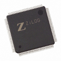
EZ80F92AZ020EG Zilog, EZ80F92AZ020EG Datasheet - Page 57

EZ80F92AZ020EG
Manufacturer Part Number
EZ80F92AZ020EG
Description
IC ACCLAIM MCU 128KB 100LQFP
Manufacturer
Zilog
Series
eZ80® Acclaim!®r
Specifications of EZ80F92AZ020EG
Core Processor
Z8
Core Size
8-Bit
Speed
20MHz
Connectivity
I²C, IrDA, SPI, UART/USART
Peripherals
Brown-out Detect/Reset, POR, WDT
Number Of I /o
24
Program Memory Size
128KB (128K x 8)
Program Memory Type
FLASH
Ram Size
8K x 8
Voltage - Supply (vcc/vdd)
3 V ~ 3.6 V
Oscillator Type
Internal
Operating Temperature
-40°C ~ 105°C
Package / Case
100-LQFP
Processor Series
EZ80F92x
Core
eZ80
Data Bus Width
8 bit
Data Ram Size
8 KB
Interface Type
I2C, IrDA, SPI, UART
Maximum Clock Frequency
20 MHz
Number Of Programmable I/os
24
Number Of Timers
6
Operating Supply Voltage
3 V to 3.6 V
Maximum Operating Temperature
+ 105 C
Mounting Style
SMD/SMT
Development Tools By Supplier
eZ80F920200ZCOG
Minimum Operating Temperature
- 40 C
Lead Free Status / RoHS Status
Lead free / RoHS Compliant
Eeprom Size
-
Data Converters
-
Lead Free Status / Rohs Status
Details
Other names
269-3871
EZ80F92AZ020EG
EZ80F92AZ020EG
Available stocks
Company
Part Number
Manufacturer
Quantity
Price
- Current page: 57 of 261
- Download datasheet (4Mb)
Table 13. Register Values for Memory Chip Select Example in Figure 6
PS015313-0508
Chip
Select
CS0
CS1
CS2
CS3
I/O Chip Select Operation
CSx_CTL[3]
CSx_EN
1
1
1
1
I/O Chip Selects can only be active when the CPU is performing I/O instructions. Because
the I/O space is separate from the memory space in the eZ80F92 device, there can never
be a conflict between I/O and memory addresses.
The eZ80F92 device supports a 16-bit I/O address. The I/O Chip Select logic decodes the
High byte of the I/O address, ADDR[15:8]. Because the upper byte of the address bus,
ADDR[23:16], is ignored, the I/O devices can always be accessed from within any mem-
ory mode (ADL or Z80
mode page is also always ignored.
Four I/O Chip Selects are available with the eZ80F92 device. To generate a particular I/O
Chip Select, the following conditions must be met:
•
•
•
•
•
•
The Chip Select is enabled by setting CSX_EN to 1
The Chip Select is configured for I/O by setting CSX_IO to 1
An I/O Chip Select address match occurs—ADDR[15:8] = CSx_LBR[7:0]
No higher-priority (lower-number) Chip Select meets the above conditions
The I/O address is not within the on-chip peripheral address range
On-chip peripheral registers assume priority for all addresses where:
0080h ≤ ADDR[15:0] ≤ 00FFh
An I/O instruction must be executing
CSx_CTL[4]
CSx_IO
0
0
0
0
CSx_LBR CSx_UBR Description
®
A0h
D0h
00h
00h
). The MBASE offset value used for setting the Z80 MEMORY
CFh
FFh
7Fh
9Fh
CS0 is enabled as a Memory Chip Select.
Valid addresses range from 000000h–
7FFFFFh.
CS1 is enabled as a Memory Chip Select.
Valid addresses range from 800000h–
9FFFFFh.
CS2 is enabled as a Memory Chip Select.
Valid addresses range from A00000h–
CFFFFFh.
CS3 is enabled as a Memory Chip Select.
Valid addresses range from D00000h–
FFFFFFh.
Chip Selects and Wait States
Product Specification
eZ80F92/eZ80F93
0080h
–
00FFh
.
50
Related parts for EZ80F92AZ020EG
Image
Part Number
Description
Manufacturer
Datasheet
Request
R

Part Number:
Description:
Communication Controllers, ZILOG INTELLIGENT PERIPHERAL CONTROLLER (ZIP)
Manufacturer:
Zilog, Inc.
Datasheet:

Part Number:
Description:
KIT DEV FOR Z8 ENCORE 16K TO 64K
Manufacturer:
Zilog
Datasheet:

Part Number:
Description:
KIT DEV Z8 ENCORE XP 28-PIN
Manufacturer:
Zilog
Datasheet:

Part Number:
Description:
DEV KIT FOR Z8 ENCORE 8K/4K
Manufacturer:
Zilog
Datasheet:

Part Number:
Description:
KIT DEV Z8 ENCORE XP 28-PIN
Manufacturer:
Zilog
Datasheet:

Part Number:
Description:
DEV KIT FOR Z8 ENCORE 4K TO 8K
Manufacturer:
Zilog
Datasheet:

Part Number:
Description:
CMOS Z8 microcontroller. ROM 16 Kbytes, RAM 256 bytes, speed 16 MHz, 32 lines I/O, 3.0V to 5.5V
Manufacturer:
Zilog, Inc.
Datasheet:

Part Number:
Description:
Low-cost microcontroller. 512 bytes ROM, 61 bytes RAM, 8 MHz
Manufacturer:
Zilog, Inc.
Datasheet:

Part Number:
Description:
Z8 4K OTP Microcontroller
Manufacturer:
Zilog, Inc.
Datasheet:

Part Number:
Description:
CMOS SUPER8 ROMLESS MCU
Manufacturer:
Zilog, Inc.
Datasheet:

Part Number:
Description:
SL1866 CMOSZ8 OTP Microcontroller
Manufacturer:
Zilog, Inc.
Datasheet:

Part Number:
Description:
SL1866 CMOSZ8 OTP Microcontroller
Manufacturer:
Zilog, Inc.
Datasheet:

Part Number:
Description:
OTP (KB) = 1, RAM = 125, Speed = 12, I/O = 14, 8-bit Timers = 2, Comm Interfaces Other Features = Por, LV Protect, Voltage = 4.5-5.5V
Manufacturer:
Zilog, Inc.
Datasheet:

Part Number:
Description:
Manufacturer:
Zilog, Inc.
Datasheet:


