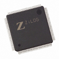
EZ80F92AZ020EG Zilog, EZ80F92AZ020EG Datasheet - Page 74

EZ80F92AZ020EG
Manufacturer Part Number
EZ80F92AZ020EG
Description
IC ACCLAIM MCU 128KB 100LQFP
Manufacturer
Zilog
Series
eZ80® Acclaim!®r
Specifications of EZ80F92AZ020EG
Core Processor
Z8
Core Size
8-Bit
Speed
20MHz
Connectivity
I²C, IrDA, SPI, UART/USART
Peripherals
Brown-out Detect/Reset, POR, WDT
Number Of I /o
24
Program Memory Size
128KB (128K x 8)
Program Memory Type
FLASH
Ram Size
8K x 8
Voltage - Supply (vcc/vdd)
3 V ~ 3.6 V
Oscillator Type
Internal
Operating Temperature
-40°C ~ 105°C
Package / Case
100-LQFP
Processor Series
EZ80F92x
Core
eZ80
Data Bus Width
8 bit
Data Ram Size
8 KB
Interface Type
I2C, IrDA, SPI, UART
Maximum Clock Frequency
20 MHz
Number Of Programmable I/os
24
Number Of Timers
6
Operating Supply Voltage
3 V to 3.6 V
Maximum Operating Temperature
+ 105 C
Mounting Style
SMD/SMT
Development Tools By Supplier
eZ80F920200ZCOG
Minimum Operating Temperature
- 40 C
Lead Free Status / RoHS Status
Lead free / RoHS Compliant
Eeprom Size
-
Data Converters
-
Lead Free Status / Rohs Status
Details
Other names
269-3871
EZ80F92AZ020EG
EZ80F92AZ020EG
Available stocks
Company
Part Number
Manufacturer
Quantity
Price
- Current page: 74 of 261
- Download datasheet (4Mb)
Table 22. Chip Select x Lower Bound Register(CS0_LBR = 00A8h, CS1_LBR = 00ABh, CS2_LBR =
PS015313-0508
Chip Select Registers
Chip Select x Lower Bound Register
For Memory Chip Selects, the Chip Select x Lower Bound register, listed in
defines the lower bound of the address range for which the corresponding Memory Chip
Select (if enabled) can be active. For I/O Chip Selects, this register defines the address to
which ADDR[15:8] is compared to generate an I/O Chip Select. All Chip Select lower
bound registers reset to
00AEh, CS3_LBR = 00B1h)
Bit
CS0_LBR Reset
CS1_LBR Reset
CS2_LBR Reset
CS3_LBR Reset
CPU Access
Note: R/W = Read/Write.
Bit
Position
[7:0]
CSx_LBR
Value Description
00h–
FFh
For Memory Chip Selects (
This byte specifies the lower bound of the Chip Select address
range. The upper byte of the address bus, ADDR[23:16], is
compared to the values contained in these registers for
determining whether a Memory Chip Select signal should be
generated.
For I/O Chip Selects (
This byte specifies the Chip Select address value. ADDR[15:8] is
compared to the values contained in these registers for
determining whether an I/O Chip Select signal should be
generated.
00h
R/W
.
7
0
0
0
0
R/W
6
0
0
0
0
R/W
5
0
0
0
0
CSX_IO
R/W
CSX_IO
4
0
0
0
0
= 1)
R/W
3
0
0
0
0
= 0)
Chip Selects and Wait States
Product Specification
R/W
2
0
0
0
0
eZ80F92/eZ80F93
R/W
Table
1
0
0
0
0
22,
R/W
0
0
0
0
0
67
Related parts for EZ80F92AZ020EG
Image
Part Number
Description
Manufacturer
Datasheet
Request
R

Part Number:
Description:
Communication Controllers, ZILOG INTELLIGENT PERIPHERAL CONTROLLER (ZIP)
Manufacturer:
Zilog, Inc.
Datasheet:

Part Number:
Description:
KIT DEV FOR Z8 ENCORE 16K TO 64K
Manufacturer:
Zilog
Datasheet:

Part Number:
Description:
KIT DEV Z8 ENCORE XP 28-PIN
Manufacturer:
Zilog
Datasheet:

Part Number:
Description:
DEV KIT FOR Z8 ENCORE 8K/4K
Manufacturer:
Zilog
Datasheet:

Part Number:
Description:
KIT DEV Z8 ENCORE XP 28-PIN
Manufacturer:
Zilog
Datasheet:

Part Number:
Description:
DEV KIT FOR Z8 ENCORE 4K TO 8K
Manufacturer:
Zilog
Datasheet:

Part Number:
Description:
CMOS Z8 microcontroller. ROM 16 Kbytes, RAM 256 bytes, speed 16 MHz, 32 lines I/O, 3.0V to 5.5V
Manufacturer:
Zilog, Inc.
Datasheet:

Part Number:
Description:
Low-cost microcontroller. 512 bytes ROM, 61 bytes RAM, 8 MHz
Manufacturer:
Zilog, Inc.
Datasheet:

Part Number:
Description:
Z8 4K OTP Microcontroller
Manufacturer:
Zilog, Inc.
Datasheet:

Part Number:
Description:
CMOS SUPER8 ROMLESS MCU
Manufacturer:
Zilog, Inc.
Datasheet:

Part Number:
Description:
SL1866 CMOSZ8 OTP Microcontroller
Manufacturer:
Zilog, Inc.
Datasheet:

Part Number:
Description:
SL1866 CMOSZ8 OTP Microcontroller
Manufacturer:
Zilog, Inc.
Datasheet:

Part Number:
Description:
OTP (KB) = 1, RAM = 125, Speed = 12, I/O = 14, 8-bit Timers = 2, Comm Interfaces Other Features = Por, LV Protect, Voltage = 4.5-5.5V
Manufacturer:
Zilog, Inc.
Datasheet:

Part Number:
Description:
Manufacturer:
Zilog, Inc.
Datasheet:


