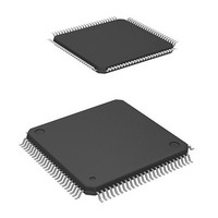
HD64F2239TF20I Renesas Electronics America, HD64F2239TF20I Datasheet - Page 116

HD64F2239TF20I
Manufacturer Part Number
HD64F2239TF20I
Description
MCU 3V 384K I-TEMP 100-TQFP
Manufacturer
Renesas Electronics America
Series
H8® H8S/2200r
Datasheet
1.DF2238RFA6V.pdf
(1048 pages)
Specifications of HD64F2239TF20I
Core Processor
H8S/2000
Core Size
16-Bit
Speed
20MHz
Connectivity
I²C, SCI, SmartCard
Peripherals
DMA, POR, PWM, WDT
Number Of I /o
72
Program Memory Size
384KB (384K x 8)
Program Memory Type
FLASH
Ram Size
32K x 8
Voltage - Supply (vcc/vdd)
2.7 V ~ 3.6 V
Data Converters
A/D 8x10b; D/A 2x8b
Oscillator Type
Internal
Operating Temperature
-40°C ~ 85°C
Package / Case
100-TQFP, 100-VQFP
Lead Free Status / RoHS Status
Contains lead / RoHS non-compliant
Eeprom Size
-
Available stocks
Company
Part Number
Manufacturer
Quantity
Price
Company:
Part Number:
HD64F2239TF20I
Manufacturer:
Renesas Electronics America
Quantity:
10 000
- Current page: 116 of 1048
- Download datasheet (6Mb)
Section 1 Overview
Type
8-bit timer
Watchdog
timer (WDT)
I
interface
(IIC)
(optional)
A/D
converter
Rev. 6.00 Mar. 18, 2010 Page 54 of 982
REJ09B0054-0600
Serial
communi-
cation
interface
(SCI)/
smart card
interface
2
C bus
Symbol
TMO3 to
TMO0
TMCI23
TMCI01
TMRI23
TMRI01
BUZZ
SCK3
SCK2
SCK1
SCK0
SCL1
SCL0
SDA1
SDA0
AN7 to
AN0
ADTRG
TxD3
TxD2
TxD1
TxD0
RxD3
RxD2
RxD1
RxD0
TFP-100B
TFP-100BV
TFP-100G
TFP-100GV
FP-100B
FP-100BV
88 to 85
89
90
89
90
74
85
33
81
78
79
81
78
80
52 to 45
72
83
31
79
76
84
32
80
77
FP-100A *
FP-100AV *
91 to 88
92
93
92
93
77
88
36
84
81
82
84
81
83
55 to 48
75
86
34
82
79
87
35
83
80
Pin No.
3
3
BP-112 *
BP-112V *
TBP-112A *
TBP-112AV *
A7, A6, B7,
C6
B6
D6
B6
D6
B11
A7
L4
B8
B9
A9
B8
B9
C8
L10, L9,
K11, K10,
K9, K8, J8,
H7
D9
D7
J4
A9
A10
C7
K4
C8
D8
1
1
4
4
I/O
Output
Input
Input
Output
Input/
Output
Input/
Output
Input/
Output
Input
Input
Output
Input
Function
Compare-match output pins.
Pins for external clock input to the counter.
Counter reset input pins.
This pin outputs the pulse that is divided
by watchdog timer.
Clock input/output pins. SCK1 outputs
NMOS push/pull.
I
drive bus. The output of SCL0 is NMOS
open drain.
I
drive bus. The output of SDA0 is NMOS
open drain.
Analog input pins for the A/D converter.
Pin for input of an external trigger to start
A/D conversion.
Data output pins.
Data input pins.
2
2
C clock input/output pins. These pins
C data input/output pins. These pins
Related parts for HD64F2239TF20I
Image
Part Number
Description
Manufacturer
Datasheet
Request
R

Part Number:
Description:
KIT STARTER FOR M16C/29
Manufacturer:
Renesas Electronics America
Datasheet:

Part Number:
Description:
KIT STARTER FOR R8C/2D
Manufacturer:
Renesas Electronics America
Datasheet:

Part Number:
Description:
R0K33062P STARTER KIT
Manufacturer:
Renesas Electronics America
Datasheet:

Part Number:
Description:
KIT STARTER FOR R8C/23 E8A
Manufacturer:
Renesas Electronics America
Datasheet:

Part Number:
Description:
KIT STARTER FOR R8C/25
Manufacturer:
Renesas Electronics America
Datasheet:

Part Number:
Description:
KIT STARTER H8S2456 SHARPE DSPLY
Manufacturer:
Renesas Electronics America
Datasheet:

Part Number:
Description:
KIT STARTER FOR R8C38C
Manufacturer:
Renesas Electronics America
Datasheet:

Part Number:
Description:
KIT STARTER FOR R8C35C
Manufacturer:
Renesas Electronics America
Datasheet:

Part Number:
Description:
KIT STARTER FOR R8CL3AC+LCD APPS
Manufacturer:
Renesas Electronics America
Datasheet:

Part Number:
Description:
KIT STARTER FOR RX610
Manufacturer:
Renesas Electronics America
Datasheet:

Part Number:
Description:
KIT STARTER FOR R32C/118
Manufacturer:
Renesas Electronics America
Datasheet:

Part Number:
Description:
KIT DEV RSK-R8C/26-29
Manufacturer:
Renesas Electronics America
Datasheet:

Part Number:
Description:
KIT STARTER FOR SH7124
Manufacturer:
Renesas Electronics America
Datasheet:

Part Number:
Description:
KIT STARTER FOR H8SX/1622
Manufacturer:
Renesas Electronics America
Datasheet:

Part Number:
Description:
KIT DEV FOR SH7203
Manufacturer:
Renesas Electronics America
Datasheet:


