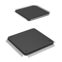
HD64F2239TF20I Renesas Electronics America, HD64F2239TF20I Datasheet - Page 434

HD64F2239TF20I
Manufacturer Part Number
HD64F2239TF20I
Description
MCU 3V 384K I-TEMP 100-TQFP
Manufacturer
Renesas Electronics America
Series
H8® H8S/2200r
Datasheet
1.DF2238RFA6V.pdf
(1048 pages)
Specifications of HD64F2239TF20I
Core Processor
H8S/2000
Core Size
16-Bit
Speed
20MHz
Connectivity
I²C, SCI, SmartCard
Peripherals
DMA, POR, PWM, WDT
Number Of I /o
72
Program Memory Size
384KB (384K x 8)
Program Memory Type
FLASH
Ram Size
32K x 8
Voltage - Supply (vcc/vdd)
2.7 V ~ 3.6 V
Data Converters
A/D 8x10b; D/A 2x8b
Oscillator Type
Internal
Operating Temperature
-40°C ~ 85°C
Package / Case
100-TQFP, 100-VQFP
Lead Free Status / RoHS Status
Contains lead / RoHS non-compliant
Eeprom Size
-
Available stocks
Company
Part Number
Manufacturer
Quantity
Price
Company:
Part Number:
HD64F2239TF20I
Manufacturer:
Renesas Electronics America
Quantity:
10 000
- Current page: 434 of 1048
- Download datasheet (6Mb)
Section 11 16-Bit Timer Pulse Unit (TPU)
11.3.2
The TMDR registers are used to set the operating mode for each channel. The TPU of the
H8S/2227 Group has a total of three TMDR registers, one each for channels 0 to 2. In other
groups, the TPU has a total of six TMDR registers, one each for channels 0 to 5. TMDR register
settings should be made only when TCNT operation is stopped.
Note:
Rev. 6.00 Mar. 18, 2010 Page 372 of 982
REJ09B0054-0600
Bit
7, 6
5
4
3
2
1
0
* Not available in the H8S/2227 Group.
Bit Name
—
BFB
BFA
MD3
MD2
MD1
MD0
Timer Mode Register (TMDR)
Initial Value
All 1
0
0
0
0
0
0
R/W
—
R/W
R/W
R/W
R/W
R/W
R/W
Description
Reserved
These bits are always read as 1 and cannot be
modified.
Buffer Operation B
Specifies whether TGRB is to operate in the normal
way, or TGRB and TGRD are to be used together for
buffer operation. When TGRD is used as a buffer
register, TGRD input capture/output compare is not
generated.
In channels 1, 2, 4 * , and 5 * , which have no TGRD,
bit 5 is reserved. It is always read as 0 and cannot be
modified.
0: TGRB operates normally
1: TGRB and TGRD used together for buffer
Buffer Operation A
Specifies whether TGRA is to operate in the normal
way, or TGRA and TGRC are to be used together for
buffer operation. When TGRC is used as a buffer
register, TGRC input capture/output compare is not
generated.
In channels 1, 2, 4 * , and 5 * , which have no TGRC,
bit 4 is reserved. It is always read as 0 and cannot be
modified.
0: TGRA operates normally
1: TGRA and TGRC used together for buffer
Modes 3 to 0
These bits are used to set the timer operating mode.
MD3 is a reserved bit. The write value should always
be 0. See table 11.11 for details.
operation
operation
Related parts for HD64F2239TF20I
Image
Part Number
Description
Manufacturer
Datasheet
Request
R

Part Number:
Description:
KIT STARTER FOR M16C/29
Manufacturer:
Renesas Electronics America
Datasheet:

Part Number:
Description:
KIT STARTER FOR R8C/2D
Manufacturer:
Renesas Electronics America
Datasheet:

Part Number:
Description:
R0K33062P STARTER KIT
Manufacturer:
Renesas Electronics America
Datasheet:

Part Number:
Description:
KIT STARTER FOR R8C/23 E8A
Manufacturer:
Renesas Electronics America
Datasheet:

Part Number:
Description:
KIT STARTER FOR R8C/25
Manufacturer:
Renesas Electronics America
Datasheet:

Part Number:
Description:
KIT STARTER H8S2456 SHARPE DSPLY
Manufacturer:
Renesas Electronics America
Datasheet:

Part Number:
Description:
KIT STARTER FOR R8C38C
Manufacturer:
Renesas Electronics America
Datasheet:

Part Number:
Description:
KIT STARTER FOR R8C35C
Manufacturer:
Renesas Electronics America
Datasheet:

Part Number:
Description:
KIT STARTER FOR R8CL3AC+LCD APPS
Manufacturer:
Renesas Electronics America
Datasheet:

Part Number:
Description:
KIT STARTER FOR RX610
Manufacturer:
Renesas Electronics America
Datasheet:

Part Number:
Description:
KIT STARTER FOR R32C/118
Manufacturer:
Renesas Electronics America
Datasheet:

Part Number:
Description:
KIT DEV RSK-R8C/26-29
Manufacturer:
Renesas Electronics America
Datasheet:

Part Number:
Description:
KIT STARTER FOR SH7124
Manufacturer:
Renesas Electronics America
Datasheet:

Part Number:
Description:
KIT STARTER FOR H8SX/1622
Manufacturer:
Renesas Electronics America
Datasheet:

Part Number:
Description:
KIT DEV FOR SH7203
Manufacturer:
Renesas Electronics America
Datasheet:


