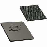
EP1S40B956C5 Altera, EP1S40B956C5 Datasheet - Page 128

EP1S40B956C5
Manufacturer Part Number
EP1S40B956C5
Description
IC STRATIX FPGA 40K LE 956-BGA
Manufacturer
Altera
Series
Stratix®r
Datasheet
1.EP1S10F484I6N.pdf
(864 pages)
Specifications of EP1S40B956C5
Number Of Logic Elements/cells
41250
Number Of Labs/clbs
4125
Total Ram Bits
3423744
Number Of I /o
683
Voltage - Supply
1.425 V ~ 1.575 V
Mounting Type
Surface Mount
Operating Temperature
0°C ~ 85°C
Package / Case
956-BGA
Lead Free Status / RoHS Status
Contains lead / RoHS non-compliant
Number Of Gates
-
Available stocks
Company
Part Number
Manufacturer
Quantity
Price
Part Number:
EP1S40B956C5
Manufacturer:
ALTERA/阿尔特拉
Quantity:
20 000
- Current page: 128 of 864
- Download datasheet (11Mb)
I/O Structure
I/O Structure
2–104
Stratix Device Handbook, Volume 1
Control Signals
The fast PLL has the same lock output, pllenable input, and areset
input control signals as the enhanced PLL.
If the input clock stops and causes the PLL to lose lock, then the PLL must
be reset for correct phase shift operation.
For more information on high-speed differential I/O support, see
Speed Differential I/O Support” on page
IOEs provide many features, including:
■
■
■
■
■
■
■
■
■
■
■
■
■
■
■
The IOE in Stratix devices contains a bidirectional I/O buffer, six
registers, and a latch for a complete embedded bidirectional single data
rate or DDR transfer.
IOE contains two input registers (plus a latch), two output registers, and
two output enable registers. The design can use both input registers and
the latch to capture DDR input and both output registers to drive DDR
outputs. Additionally, the design can use the output enable (OE) register
for fast clock-to-output enable timing. The negative edge-clocked OE
register is used for DDR SDRAM interfacing. The Quartus II software
automatically duplicates a single OE register that controls multiple
output or bidirectional pins.
Dedicated differential and single-ended I/O buffers
3.3-V, 64-bit, 66-MHz PCI compliance
3.3-V, 64-bit, 133-MHz PCI-X 1.0 compliance
Joint Test Action Group (JTAG) boundary-scan test (BST) support
Differential on-chip termination for LVDS I/O standard
Programmable pull-up during configuration
Output drive strength control
Slew-rate control
Tri-state buffers
Bus-hold circuitry
Programmable pull-up resistors
Programmable input and output delays
Open-drain outputs
DQ and DQS I/O pins
Double-data rate (DDR) Registers
Figure 2–59
shows the Stratix IOE structure. The
2–130.
Altera Corporation
July 2005
“High-
Related parts for EP1S40B956C5
Image
Part Number
Description
Manufacturer
Datasheet
Request
R

Part Number:
Description:
CYCLONE II STARTER KIT EP2C20N
Manufacturer:
Altera
Datasheet:

Part Number:
Description:
CPLD, EP610 Family, ECMOS Process, 300 Gates, 16 Macro Cells, 16 Reg., 16 User I/Os, 5V Supply, 35 Speed Grade, 24DIP
Manufacturer:
Altera Corporation
Datasheet:

Part Number:
Description:
CPLD, EP610 Family, ECMOS Process, 300 Gates, 16 Macro Cells, 16 Reg., 16 User I/Os, 5V Supply, 15 Speed Grade, 24DIP
Manufacturer:
Altera Corporation
Datasheet:

Part Number:
Description:
Manufacturer:
Altera Corporation
Datasheet:

Part Number:
Description:
CPLD, EP610 Family, ECMOS Process, 300 Gates, 16 Macro Cells, 16 Reg., 16 User I/Os, 5V Supply, 30 Speed Grade, 24DIP
Manufacturer:
Altera Corporation
Datasheet:

Part Number:
Description:
High-performance, low-power erasable programmable logic devices with 8 macrocells, 10ns
Manufacturer:
Altera Corporation
Datasheet:

Part Number:
Description:
High-performance, low-power erasable programmable logic devices with 8 macrocells, 7ns
Manufacturer:
Altera Corporation
Datasheet:

Part Number:
Description:
Classic EPLD
Manufacturer:
Altera Corporation
Datasheet:

Part Number:
Description:
High-performance, low-power erasable programmable logic devices with 8 macrocells, 10ns
Manufacturer:
Altera Corporation
Datasheet:

Part Number:
Description:
Manufacturer:
Altera Corporation
Datasheet:

Part Number:
Description:
Manufacturer:
Altera Corporation
Datasheet:

Part Number:
Description:
Manufacturer:
Altera Corporation
Datasheet:

Part Number:
Description:
CPLD, EP610 Family, ECMOS Process, 300 Gates, 16 Macro Cells, 16 Reg., 16 User I/Os, 5V Supply, 25 Speed Grade, 24DIP
Manufacturer:
Altera Corporation
Datasheet:


