EP1S40B956C5 Altera, EP1S40B956C5 Datasheet - Page 804
EP1S40B956C5
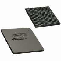
Manufacturer Part Number
EP1S40B956C5
Description
IC STRATIX FPGA 40K LE 956-BGA
Manufacturer
Altera
Series
Stratix®r
Datasheet
1.EP1S10F484I6N.pdf
(864 pages)
Specifications of EP1S40B956C5
Number Of Logic Elements/cells
41250
Number Of Labs/clbs
4125
Total Ram Bits
3423744
Number Of I /o
683
Voltage - Supply
1.425 V ~ 1.575 V
Mounting Type
Surface Mount
Operating Temperature
0°C ~ 85°C
Package / Case
956-BGA
Lead Free Status / RoHS Status
Contains lead / RoHS non-compliant
Number Of Gates
-
Available stocks
Company
Part Number
Manufacturer
Quantity
Price

Part Number:
EP1S40B956C5
Manufacturer:
ALTERA/阿尔特拉
Quantity:
20 000


Using Enhanced Configuration Devices
12–26
Stratix Device Handbook, Volume 2
3.
4.
5.
6.
7.
8.
9.
10. Click OK to generate initial programming and memory map files.
Select the enhanced configuration device (EPC4, EPC8, EPC16), and
the mode used (1-bit Passive Serial or Fast Passive Parallel). Only
during the initial programming file generation can you specify the
Options, Configuration device, or Mode settings. While generating
the partial programming file, all of these settings are grayed out and
inaccessible.
In the Input files to convert box, highlight SOF Data at Page 0 and
click Add File. Select input SOF file(s) for this configuration page
and insert them.
Repeat Step 4 for the Page 1 application configuration page.
For enabling block addressing, select the SOF Data entry for Page 1,
and click Properties. This opens the SOF Data Properties dialog
box (see
Pick Block from the Address Mode drop down selection, and enter
32-bit Hexadecimal byte address for block Starting Address and
Ending Address. Note that for partial programming support, the
block start and end addresses should be aligned to a flash sector
boundary. This prevents two configuration pages from overlapping
within the same flash boundary. See the flash memory datasheet for
data sector boundary information. Click OK to save SOF data
properties.
Check the Memory Map File box to generate a memory map output
file that specifies the start/end addresses of each configuration page
and user data blocks.
Save the CPF setup (optionally), by selecting Save Conversion
Setup… and specifying a name for the COF output file.
Figure
12–15).
Altera Corporation
September 2004
Related parts for EP1S40B956C5
Image
Part Number
Description
Manufacturer
Datasheet
Request
R

Part Number:
Description:
CYCLONE II STARTER KIT EP2C20N
Manufacturer:
Altera
Datasheet:


Part Number:
Description:
CPLD, EP610 Family, ECMOS Process, 300 Gates, 16 Macro Cells, 16 Reg., 16 User I/Os, 5V Supply, 35 Speed Grade, 24DIP
Manufacturer:
Altera Corporation
Datasheet:
Part Number:
Description:
CPLD, EP610 Family, ECMOS Process, 300 Gates, 16 Macro Cells, 16 Reg., 16 User I/Os, 5V Supply, 15 Speed Grade, 24DIP
Manufacturer:
Altera Corporation
Datasheet:
Part Number:
Description:
Manufacturer:
Altera Corporation
Datasheet:
Part Number:
Description:
CPLD, EP610 Family, ECMOS Process, 300 Gates, 16 Macro Cells, 16 Reg., 16 User I/Os, 5V Supply, 30 Speed Grade, 24DIP
Manufacturer:
Altera Corporation
Datasheet:
Part Number:
Description:
High-performance, low-power erasable programmable logic devices with 8 macrocells, 10ns
Manufacturer:
Altera Corporation
Datasheet:
Part Number:
Description:
High-performance, low-power erasable programmable logic devices with 8 macrocells, 7ns
Manufacturer:
Altera Corporation
Datasheet:
Part Number:
Description:
Classic EPLD
Manufacturer:
Altera Corporation
Datasheet:
Part Number:
Description:
High-performance, low-power erasable programmable logic devices with 8 macrocells, 10ns
Manufacturer:
Altera Corporation
Datasheet:
Part Number:
Description:
Manufacturer:
Altera Corporation
Datasheet:
Part Number:
Description:
Manufacturer:
Altera Corporation
Datasheet:
Part Number:
Description:
Manufacturer:
Altera Corporation
Datasheet:
Part Number:
Description:
CPLD, EP610 Family, ECMOS Process, 300 Gates, 16 Macro Cells, 16 Reg., 16 User I/Os, 5V Supply, 25 Speed Grade, 24DIP
Manufacturer:
Altera Corporation
Datasheet: