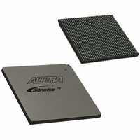
EP1S40B956C5 Altera, EP1S40B956C5 Datasheet - Page 659

EP1S40B956C5
Manufacturer Part Number
EP1S40B956C5
Description
IC STRATIX FPGA 40K LE 956-BGA
Manufacturer
Altera
Series
Stratix®r
Datasheet
1.EP1S10F484I6N.pdf
(864 pages)
Specifications of EP1S40B956C5
Number Of Logic Elements/cells
41250
Number Of Labs/clbs
4125
Total Ram Bits
3423744
Number Of I /o
683
Voltage - Supply
1.425 V ~ 1.575 V
Mounting Type
Surface Mount
Operating Temperature
0°C ~ 85°C
Package / Case
956-BGA
Lead Free Status / RoHS Status
Contains lead / RoHS non-compliant
Number Of Gates
-
Available stocks
Company
Part Number
Manufacturer
Quantity
Price
Part Number:
EP1S40B956C5
Manufacturer:
ALTERA/阿尔特拉
Quantity:
20 000
- Current page: 659 of 864
- Download datasheet (11Mb)
Figure 8–11. Stratix & Stratix GX XGMII Implementation
Altera Corporation
July 2005
Stratix & Stratix GX PCS
Logic Array
Stratix GX
Stratix &
Data
Data
Clk
Clk
Receiver
Transmitter
DDR Output Circuitry
DDR Input Circuitry
For this implementation, the shift register clocks can either be generated
from a divided down MAC reconciliation sublayer transmitter clock
(MAC_TXCLK), or the asynchronous core clock, or both if using a FIFO
buffer.
Figure 8–12
transmitted from the PCS to the MAC reconciliation sublayer starts at the
core of the Stratix or Stratix GX device and travels to the shift register. The
shift register takes in the parallel data (even bits sent to the top register
and odd bits sent to the bottom register) and serializes the data. After the
data is serialized, it travels to the double data rate (DDR) output circuitry,
which is clocked with the 4 clock from the PLL. Out of the DDR output
circuitry, the data drives off-chip along with the 4 clock. This transaction
creates the DDR relationship between the clock and the data output. This
implementation only shows one channel, but can be duplicated to include
all 32 bits of the RX_D signal and all 4 bits of the RX_C signal.
PLL2
Register
Register
Shift
÷4
Shift
Implementing 10-Gigabit Ethernet Using Stratix & Stratix GX Devices
PLL1
shows one channel of the output half of XGMII. Data that is
×4
MAC_RXCLK
MAC_TXCLK
RX_D[31..0]
TX_D[31..0]
RX_C[3..0]
TX_C[3..0]
Stratix Device Handbook, Volume 2
MAC (RS)
Transmitter
Receiver
8–15
Related parts for EP1S40B956C5
Image
Part Number
Description
Manufacturer
Datasheet
Request
R

Part Number:
Description:
CYCLONE II STARTER KIT EP2C20N
Manufacturer:
Altera
Datasheet:

Part Number:
Description:
CPLD, EP610 Family, ECMOS Process, 300 Gates, 16 Macro Cells, 16 Reg., 16 User I/Os, 5V Supply, 35 Speed Grade, 24DIP
Manufacturer:
Altera Corporation
Datasheet:

Part Number:
Description:
CPLD, EP610 Family, ECMOS Process, 300 Gates, 16 Macro Cells, 16 Reg., 16 User I/Os, 5V Supply, 15 Speed Grade, 24DIP
Manufacturer:
Altera Corporation
Datasheet:

Part Number:
Description:
Manufacturer:
Altera Corporation
Datasheet:

Part Number:
Description:
CPLD, EP610 Family, ECMOS Process, 300 Gates, 16 Macro Cells, 16 Reg., 16 User I/Os, 5V Supply, 30 Speed Grade, 24DIP
Manufacturer:
Altera Corporation
Datasheet:

Part Number:
Description:
High-performance, low-power erasable programmable logic devices with 8 macrocells, 10ns
Manufacturer:
Altera Corporation
Datasheet:

Part Number:
Description:
High-performance, low-power erasable programmable logic devices with 8 macrocells, 7ns
Manufacturer:
Altera Corporation
Datasheet:

Part Number:
Description:
Classic EPLD
Manufacturer:
Altera Corporation
Datasheet:

Part Number:
Description:
High-performance, low-power erasable programmable logic devices with 8 macrocells, 10ns
Manufacturer:
Altera Corporation
Datasheet:

Part Number:
Description:
Manufacturer:
Altera Corporation
Datasheet:

Part Number:
Description:
Manufacturer:
Altera Corporation
Datasheet:

Part Number:
Description:
Manufacturer:
Altera Corporation
Datasheet:

Part Number:
Description:
CPLD, EP610 Family, ECMOS Process, 300 Gates, 16 Macro Cells, 16 Reg., 16 User I/Os, 5V Supply, 25 Speed Grade, 24DIP
Manufacturer:
Altera Corporation
Datasheet:


