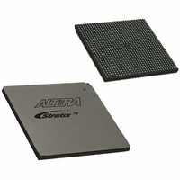
EP1S40B956C5 Altera, EP1S40B956C5 Datasheet - Page 378

EP1S40B956C5
Manufacturer Part Number
EP1S40B956C5
Description
IC STRATIX FPGA 40K LE 956-BGA
Manufacturer
Altera
Series
Stratix®r
Datasheet
1.EP1S10F484I6N.pdf
(864 pages)
Specifications of EP1S40B956C5
Number Of Logic Elements/cells
41250
Number Of Labs/clbs
4125
Total Ram Bits
3423744
Number Of I /o
683
Voltage - Supply
1.425 V ~ 1.575 V
Mounting Type
Surface Mount
Operating Temperature
0°C ~ 85°C
Package / Case
956-BGA
Lead Free Status / RoHS Status
Contains lead / RoHS non-compliant
Number Of Gates
-
Available stocks
Company
Part Number
Manufacturer
Quantity
Price
Part Number:
EP1S40B956C5
Manufacturer:
ALTERA/阿尔特拉
Quantity:
20 000
- Current page: 378 of 864
- Download datasheet (11Mb)
Using TriMatrix Memory
2–10
Stratix Device Handbook, Volume 2
128
512
256
128
64K
32K
16K
8K
4K
Table 2–8. M4K Block Mixed-Width Configurations (Simple Dual-Port Mode) (Part 2 of 2)
Table 2–9. M-RAM Block Mixed-Width Configurations (Simple Dual-Port Mode)
Read Port
72
144
32
9
18
36
9
18
36
Read Port
4K
f
v
1 2K
v
M512 blocks support serializer and deserializer (SERDES) applications.
By using the mixed-width support in combination with double data rate
(DDR) I/O standards, the block can function as a SERDES to support low-
speed serial I/O standards using global or regional clocks.
For more information on Stratix device I/O structure see the Stratix
Device Family Data Sheet section of the Stratix Device Handbook, Volume 1.
For more information on Stratix GX device I/O structure see the
Stratix GX Device Family Data Sheet section of the Stratix GX Device
Handbook, Volume 1.
In simple dual-port mode, the M512 and M4K blocks have one write
enable and one read enable signal. The M512 does not support a clear port
on the rden register. On the M4K block, asserting the clear port of the
rden register drives rden high, which allows the read operation to occur.
When the read enable is deactivated, the current data is retained at the
output ports. If the read enable is activated during a write operation with
the same address location selected, the simple dual-port RAM output is
either unknown or can be set to output the old data stored at the memory
address. For more information, see
Same Address” on page
2 1K
64K
v
v
v
v
v
4 512
9
v
32K
8 256
v
v
v
v
18
2–25.
Write Port
v
16 128
Write Port
16K
“Read-During-Write Operation at the
v
v
v
v
v
36
32 512
v
v
v
8K
9 256
v
v
v
v
72
Altera Corporation
v
v
v
18 128
4K
July 2005
v
v
v
v
144
36
Related parts for EP1S40B956C5
Image
Part Number
Description
Manufacturer
Datasheet
Request
R

Part Number:
Description:
CYCLONE II STARTER KIT EP2C20N
Manufacturer:
Altera
Datasheet:

Part Number:
Description:
CPLD, EP610 Family, ECMOS Process, 300 Gates, 16 Macro Cells, 16 Reg., 16 User I/Os, 5V Supply, 35 Speed Grade, 24DIP
Manufacturer:
Altera Corporation
Datasheet:

Part Number:
Description:
CPLD, EP610 Family, ECMOS Process, 300 Gates, 16 Macro Cells, 16 Reg., 16 User I/Os, 5V Supply, 15 Speed Grade, 24DIP
Manufacturer:
Altera Corporation
Datasheet:

Part Number:
Description:
Manufacturer:
Altera Corporation
Datasheet:

Part Number:
Description:
CPLD, EP610 Family, ECMOS Process, 300 Gates, 16 Macro Cells, 16 Reg., 16 User I/Os, 5V Supply, 30 Speed Grade, 24DIP
Manufacturer:
Altera Corporation
Datasheet:

Part Number:
Description:
High-performance, low-power erasable programmable logic devices with 8 macrocells, 10ns
Manufacturer:
Altera Corporation
Datasheet:

Part Number:
Description:
High-performance, low-power erasable programmable logic devices with 8 macrocells, 7ns
Manufacturer:
Altera Corporation
Datasheet:

Part Number:
Description:
Classic EPLD
Manufacturer:
Altera Corporation
Datasheet:

Part Number:
Description:
High-performance, low-power erasable programmable logic devices with 8 macrocells, 10ns
Manufacturer:
Altera Corporation
Datasheet:

Part Number:
Description:
Manufacturer:
Altera Corporation
Datasheet:

Part Number:
Description:
Manufacturer:
Altera Corporation
Datasheet:

Part Number:
Description:
Manufacturer:
Altera Corporation
Datasheet:

Part Number:
Description:
CPLD, EP610 Family, ECMOS Process, 300 Gates, 16 Macro Cells, 16 Reg., 16 User I/Os, 5V Supply, 25 Speed Grade, 24DIP
Manufacturer:
Altera Corporation
Datasheet:


