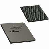
EP1S40B956C5 Altera, EP1S40B956C5 Datasheet - Page 290

EP1S40B956C5
Manufacturer Part Number
EP1S40B956C5
Description
IC STRATIX FPGA 40K LE 956-BGA
Manufacturer
Altera
Series
Stratix®r
Datasheet
1.EP1S10F484I6N.pdf
(864 pages)
Specifications of EP1S40B956C5
Number Of Logic Elements/cells
41250
Number Of Labs/clbs
4125
Total Ram Bits
3423744
Number Of I /o
683
Voltage - Supply
1.425 V ~ 1.575 V
Mounting Type
Surface Mount
Operating Temperature
0°C ~ 85°C
Package / Case
956-BGA
Lead Free Status / RoHS Status
Contains lead / RoHS non-compliant
Number Of Gates
-
Available stocks
Company
Part Number
Manufacturer
Quantity
Price
Part Number:
EP1S40B956C5
Manufacturer:
ALTERA/阿尔特拉
Quantity:
20 000
- Current page: 290 of 864
- Download datasheet (11Mb)
EP1S60 Devices
EP1S80 Devices
H
HSTL
Index–4
Column Pin
M-RAM
Row Pin
Column Pin
Global
Row Pin
Class I Specifications 4–14,
Class II Specifications 4–14,
Fast Regional Clock External I/O Timing
Global
Regional Clock External I/O Timing
Fast Regional Clock External I/O Timing
Global
Regional Clock External I/O Timing
Interface Locations
Fast Regional Clock External I/O Timing
Global
Regional Clock External I/O Timing
Fast Regional Clock External I/O Timing
Global
Regional Clock External I/O Timing
Fast Regional Clock External I/O Timing
Regional Clock External I/O Timing
Parameters
Parameters
Parameters
Parameters
Parameters
Parameters
Parameters
Parameters
Parameters
Parameters
Parameters
Parameters
Parameters
Parameters
Parameters
Clock
Clock
Clock
Clock
Clock
External
4–56
External
External
External
External
4–49
4–50
4–50
4–51
4–52
4–51
4–52
4–53
4–53
4–54
4–55
4–54
4–55
4–56
2–38
4–15
4–15
I/O
I/O
I/O
I/O
I/O
Timing
Timing
Timing
Timing
Timing
I
I/O
Standards
1.5-V 4–14,
1.8-V
2.5-V
3.3-V
Advanced I/O Standard Support
Column I/O Block Connection to the
Column Pin
Control Signal Selection per IOE
CTT I/O Specifications
Differential
External I/O Delay Parameters
GTL+ I/O Specifications
High-Speed
HyperTransport
I/O Banks
I/O Structure
I/O Support by Bank
IOE Structure
LVCMOS Specifications
LVDS
LVPECL Specifications
LVTTL Specifications
MultiVolt I/O Interface
MultiVolt I/O Support
Output Delay Adders for Fast Slew Rate
Output Delay Adders for Fast Slew Rate
Output Delay Adders for Slow Slew Rate
Package Options & I/O Pin Counts
Receiver Input Waveforms for Differential
Interconnect
Termination
Support
Specifications
Input
on Column Pins
on Row Pins
on Column Pins
4–13
I/O Specifications
I/O Specifications
I/O Specifications
LVDS I/O Specifications
PCI Specifications
PCML Specifications
Input Delay Adders
Stratix Device Handbook, Volume 1
Performance
2–125
4–15
2–103
LVDS
2–104
2–105
2–130
Differential
2–107
2–128
4–69
4–9
2–126
4–3
Altera Corporation
Input
4–68
4–70
on
4–8
2–130
4–16
2–129
4–3
4–10
4–9
4–4
4–4
4–3
4–66
Technology
4–8
Fast
4–66
On-Chip
4–6
2–109
2–122
1–4
PLL
I/O
Related parts for EP1S40B956C5
Image
Part Number
Description
Manufacturer
Datasheet
Request
R

Part Number:
Description:
CYCLONE II STARTER KIT EP2C20N
Manufacturer:
Altera
Datasheet:

Part Number:
Description:
CPLD, EP610 Family, ECMOS Process, 300 Gates, 16 Macro Cells, 16 Reg., 16 User I/Os, 5V Supply, 35 Speed Grade, 24DIP
Manufacturer:
Altera Corporation
Datasheet:

Part Number:
Description:
CPLD, EP610 Family, ECMOS Process, 300 Gates, 16 Macro Cells, 16 Reg., 16 User I/Os, 5V Supply, 15 Speed Grade, 24DIP
Manufacturer:
Altera Corporation
Datasheet:

Part Number:
Description:
Manufacturer:
Altera Corporation
Datasheet:

Part Number:
Description:
CPLD, EP610 Family, ECMOS Process, 300 Gates, 16 Macro Cells, 16 Reg., 16 User I/Os, 5V Supply, 30 Speed Grade, 24DIP
Manufacturer:
Altera Corporation
Datasheet:

Part Number:
Description:
High-performance, low-power erasable programmable logic devices with 8 macrocells, 10ns
Manufacturer:
Altera Corporation
Datasheet:

Part Number:
Description:
High-performance, low-power erasable programmable logic devices with 8 macrocells, 7ns
Manufacturer:
Altera Corporation
Datasheet:

Part Number:
Description:
Classic EPLD
Manufacturer:
Altera Corporation
Datasheet:

Part Number:
Description:
High-performance, low-power erasable programmable logic devices with 8 macrocells, 10ns
Manufacturer:
Altera Corporation
Datasheet:

Part Number:
Description:
Manufacturer:
Altera Corporation
Datasheet:

Part Number:
Description:
Manufacturer:
Altera Corporation
Datasheet:

Part Number:
Description:
Manufacturer:
Altera Corporation
Datasheet:

Part Number:
Description:
CPLD, EP610 Family, ECMOS Process, 300 Gates, 16 Macro Cells, 16 Reg., 16 User I/Os, 5V Supply, 25 Speed Grade, 24DIP
Manufacturer:
Altera Corporation
Datasheet:


