EP1S40B956C5 Altera, EP1S40B956C5 Datasheet - Page 420
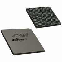
EP1S40B956C5
Manufacturer Part Number
EP1S40B956C5
Description
IC STRATIX FPGA 40K LE 956-BGA
Manufacturer
Altera
Series
Stratix®r
Datasheet
1.EP1S10F484I6N.pdf
(864 pages)
Specifications of EP1S40B956C5
Number Of Logic Elements/cells
41250
Number Of Labs/clbs
4125
Total Ram Bits
3423744
Number Of I /o
683
Voltage - Supply
1.425 V ~ 1.575 V
Mounting Type
Surface Mount
Operating Temperature
0°C ~ 85°C
Package / Case
956-BGA
Lead Free Status / RoHS Status
Contains lead / RoHS non-compliant
Number Of Gates
-
Available stocks
Company
Part Number
Manufacturer
Quantity
Price

Part Number:
EP1S40B956C5
Manufacturer:
ALTERA/阿尔特拉
Quantity:
20 000


DDR Memory Support Overview
Figure 3–13. DQS Configuration in Stratix & Stratix GX IOE
Notes to
(1)
(2)
(3)
(4)
(5)
(6)
(7)
(8)
3–24
Stratix Device Handbook, Volume 2
You can use the altdqs megafunction to generate the DQS signals.
The OE signal is active low, but the Quartus II software implements this as active high and automatically adds an
inverter before OE register A
The select line can be chosen in the altdqs MegaWizard Plug-In Manager.
The datain_l and datain_h pins are usually connected to V
DQS postamble handling is not shown in this diagram. For more information, see AN 342: Interfacing DDR SDRAM
with Stratix & Stratix GX Devices.
This undelayed DQS signal goes to the LE for the soft postamble circuitry.
You must invert this signal before it reaches the DQ IOE. This signal is automatically inverted if you use the altdq
megafunction to generate the DQ signals. Connect this port to the inclock port in the altdq megafunction.
DQS phase-shift circuitry is only available on DQS pins.
Logic Array
Figure
3–13:
datain_h (3)
(3)
datain_l (4)
system clock
OE
undelayed DQS (6)
combout (7)
OE
during compilation.
(2)
Output Register A
Output Register B
OE Register A
OE Register B
DFF
DFF
DFF
DFF
D
D
D
D
Q
Q
Q
Q
OE
OE
O
O
1
0
CC
Note (1)
and ground, respectively.
0
1
OR2
Shift Circuitry
DQS Phase
(8)
TRI
Altera Corporation
June 2006
DQS Pin (5)
Related parts for EP1S40B956C5
Image
Part Number
Description
Manufacturer
Datasheet
Request
R

Part Number:
Description:
CYCLONE II STARTER KIT EP2C20N
Manufacturer:
Altera
Datasheet:


Part Number:
Description:
CPLD, EP610 Family, ECMOS Process, 300 Gates, 16 Macro Cells, 16 Reg., 16 User I/Os, 5V Supply, 35 Speed Grade, 24DIP
Manufacturer:
Altera Corporation
Datasheet:
Part Number:
Description:
CPLD, EP610 Family, ECMOS Process, 300 Gates, 16 Macro Cells, 16 Reg., 16 User I/Os, 5V Supply, 15 Speed Grade, 24DIP
Manufacturer:
Altera Corporation
Datasheet:
Part Number:
Description:
Manufacturer:
Altera Corporation
Datasheet:
Part Number:
Description:
CPLD, EP610 Family, ECMOS Process, 300 Gates, 16 Macro Cells, 16 Reg., 16 User I/Os, 5V Supply, 30 Speed Grade, 24DIP
Manufacturer:
Altera Corporation
Datasheet:
Part Number:
Description:
High-performance, low-power erasable programmable logic devices with 8 macrocells, 10ns
Manufacturer:
Altera Corporation
Datasheet:
Part Number:
Description:
High-performance, low-power erasable programmable logic devices with 8 macrocells, 7ns
Manufacturer:
Altera Corporation
Datasheet:
Part Number:
Description:
Classic EPLD
Manufacturer:
Altera Corporation
Datasheet:
Part Number:
Description:
High-performance, low-power erasable programmable logic devices with 8 macrocells, 10ns
Manufacturer:
Altera Corporation
Datasheet:
Part Number:
Description:
Manufacturer:
Altera Corporation
Datasheet:
Part Number:
Description:
Manufacturer:
Altera Corporation
Datasheet:
Part Number:
Description:
Manufacturer:
Altera Corporation
Datasheet:
Part Number:
Description:
CPLD, EP610 Family, ECMOS Process, 300 Gates, 16 Macro Cells, 16 Reg., 16 User I/Os, 5V Supply, 25 Speed Grade, 24DIP
Manufacturer:
Altera Corporation
Datasheet: