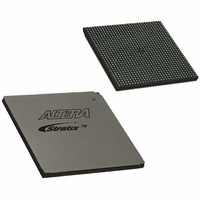
EP1S40B956C5 Altera, EP1S40B956C5 Datasheet - Page 494

EP1S40B956C5
Manufacturer Part Number
EP1S40B956C5
Description
IC STRATIX FPGA 40K LE 956-BGA
Manufacturer
Altera
Series
Stratix®r
Datasheet
1.EP1S10F484I6N.pdf
(864 pages)
Specifications of EP1S40B956C5
Number Of Logic Elements/cells
41250
Number Of Labs/clbs
4125
Total Ram Bits
3423744
Number Of I /o
683
Voltage - Supply
1.425 V ~ 1.575 V
Mounting Type
Surface Mount
Operating Temperature
0°C ~ 85°C
Package / Case
956-BGA
Lead Free Status / RoHS Status
Contains lead / RoHS non-compliant
Number Of Gates
-
Available stocks
Company
Part Number
Manufacturer
Quantity
Price
Part Number:
EP1S40B956C5
Manufacturer:
ALTERA/阿尔特拉
Quantity:
20 000
- Current page: 494 of 864
- Download datasheet (11Mb)
Differential I/O Interface & Fast PLLs
Figure 5–15. Fast PLL Connection to Logic Array
5–22
Stratix Device Handbook, Volume 2
VCO Phase Selection
Selectable at each PLL
Output Port
PLL Output
Counter Circuitry
The multiplied clocks bypass the counter taps k and v to directly feed the
SERDES serial registers. These two taps also feed to the quadrant local
clock network and the dedicated RXLOADENA or TXLOADENA pins, as
shown in
data-realignment procedure. When the design does not use the data
realignment, both TXLOADEN and RXLOADEN pins use a single counter.
The Stratix device fast PLL has another GCLK connection for general-
purpose applications. The third tap l feeds the quadrant local clock as
well as the global clock network. You can use the l counter's multiplexer
for applications requiring the device to connect the incoming clock
directly to the local or global clocks. You can program the multiplexer to
connect the RXCLKIN signal directly to the local or global clock lines.
Figure 5–15
and the local or global clock lines.
The differential clock selection is made per differential bank. Since the
length of the clock tree limits the performance, each fast PLL should drive
only one differential bank.
Counter Circuitry
8
Figure
shows the connection between the incoming clock, the l tap,
Post-Scale
clkin
Counters
5–15. Both k and v are utilized simultaneously during the
÷ k
÷ v
÷ l
Clock
Distribution
Circuitry
CLK1 SERDES
Circuitry
×1 CLK1 to logic array
or local clocks
TXLOADEN
RXLOADEN
×1 CLK2 to logic array
or local clocks
CLK2 SERDES
Circuitry
Regional clock
Altera Corporation
July 2005
Related parts for EP1S40B956C5
Image
Part Number
Description
Manufacturer
Datasheet
Request
R

Part Number:
Description:
CYCLONE II STARTER KIT EP2C20N
Manufacturer:
Altera
Datasheet:

Part Number:
Description:
CPLD, EP610 Family, ECMOS Process, 300 Gates, 16 Macro Cells, 16 Reg., 16 User I/Os, 5V Supply, 35 Speed Grade, 24DIP
Manufacturer:
Altera Corporation
Datasheet:

Part Number:
Description:
CPLD, EP610 Family, ECMOS Process, 300 Gates, 16 Macro Cells, 16 Reg., 16 User I/Os, 5V Supply, 15 Speed Grade, 24DIP
Manufacturer:
Altera Corporation
Datasheet:

Part Number:
Description:
Manufacturer:
Altera Corporation
Datasheet:

Part Number:
Description:
CPLD, EP610 Family, ECMOS Process, 300 Gates, 16 Macro Cells, 16 Reg., 16 User I/Os, 5V Supply, 30 Speed Grade, 24DIP
Manufacturer:
Altera Corporation
Datasheet:

Part Number:
Description:
High-performance, low-power erasable programmable logic devices with 8 macrocells, 10ns
Manufacturer:
Altera Corporation
Datasheet:

Part Number:
Description:
High-performance, low-power erasable programmable logic devices with 8 macrocells, 7ns
Manufacturer:
Altera Corporation
Datasheet:

Part Number:
Description:
Classic EPLD
Manufacturer:
Altera Corporation
Datasheet:

Part Number:
Description:
High-performance, low-power erasable programmable logic devices with 8 macrocells, 10ns
Manufacturer:
Altera Corporation
Datasheet:

Part Number:
Description:
Manufacturer:
Altera Corporation
Datasheet:

Part Number:
Description:
Manufacturer:
Altera Corporation
Datasheet:

Part Number:
Description:
Manufacturer:
Altera Corporation
Datasheet:

Part Number:
Description:
CPLD, EP610 Family, ECMOS Process, 300 Gates, 16 Macro Cells, 16 Reg., 16 User I/Os, 5V Supply, 25 Speed Grade, 24DIP
Manufacturer:
Altera Corporation
Datasheet:


