EP1S40B956C5 Altera, EP1S40B956C5 Datasheet - Page 774
EP1S40B956C5
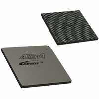
Manufacturer Part Number
EP1S40B956C5
Description
IC STRATIX FPGA 40K LE 956-BGA
Manufacturer
Altera
Series
Stratix®r
Datasheet
1.EP1S10F484I6N.pdf
(864 pages)
Specifications of EP1S40B956C5
Number Of Logic Elements/cells
41250
Number Of Labs/clbs
4125
Total Ram Bits
3423744
Number Of I /o
683
Voltage - Supply
1.425 V ~ 1.575 V
Mounting Type
Surface Mount
Operating Temperature
0°C ~ 85°C
Package / Case
956-BGA
Lead Free Status / RoHS Status
Contains lead / RoHS non-compliant
Number Of Gates
-
Available stocks
Company
Part Number
Manufacturer
Quantity
Price

Part Number:
EP1S40B956C5
Manufacturer:
ALTERA/阿尔特拉
Quantity:
20 000


Device Configuration Pins
11–56
Stratix Device Handbook, Volume 2
DATA[7..1]
DATA7
nWS
Table 11–15. Dedicated Configuration Pins on the Stratix or Stratix GX Device
Pin Name
I/O
I/O
I/O
User Mode
Parallel
configuration
schemes
(FPP and
PPA)
PPA
PPA
Configuration
Scheme
Inputs
Bidirectional In the PPA configuration scheme, the
Input
Pin Type
Data inputs. Byte-wide configuration data is
presented to the target device on
DATA[7..0]
these pins are dependent on the V
I/O banks that they reside in.
In serial configuration schemes, they function
as user I/Os during configuration, which means
they are tri-stated.
After PPA or FPP configuration,
are available as a user I/Os and the state of
these pin depends on the Dual-Purpose Pin
settings.
pin presents the
signal has been strobed low. The V
levels for this pin are dependent on the V
of the I/O bank that it resides in.
In serial configuration schemes, it functions as
a user I/O during configuration, which means it
is tri-stated.
After PPA configuration,
a user I/O and the state of this pin depends on
the Dual-Purpose Pin settings.
Write strobe input. A low-to-high transition
causes the device to latch a byte of data on the
DATA[7..0]
In non-PPA schemes, it functions as a user I/O
during configuration, which means it is tri-
stated.
After PPA configuration,
user I/O and the state of this pin depends on
the Dual-Purpose Pin settings.
. The V
pins.
RDYnBSY
Description
(Part 6 of 8)
I H
DATA7
and V
nWS
signal after the
Altera Corporation
is available as a
I L
DATA[7..1]
is available as
levels for
C C I O
I L
July 2005
and V
DATA7
of the
C C I O
nRS
I L
Related parts for EP1S40B956C5
Image
Part Number
Description
Manufacturer
Datasheet
Request
R

Part Number:
Description:
CYCLONE II STARTER KIT EP2C20N
Manufacturer:
Altera
Datasheet:


Part Number:
Description:
CPLD, EP610 Family, ECMOS Process, 300 Gates, 16 Macro Cells, 16 Reg., 16 User I/Os, 5V Supply, 35 Speed Grade, 24DIP
Manufacturer:
Altera Corporation
Datasheet:
Part Number:
Description:
CPLD, EP610 Family, ECMOS Process, 300 Gates, 16 Macro Cells, 16 Reg., 16 User I/Os, 5V Supply, 15 Speed Grade, 24DIP
Manufacturer:
Altera Corporation
Datasheet:
Part Number:
Description:
Manufacturer:
Altera Corporation
Datasheet:
Part Number:
Description:
CPLD, EP610 Family, ECMOS Process, 300 Gates, 16 Macro Cells, 16 Reg., 16 User I/Os, 5V Supply, 30 Speed Grade, 24DIP
Manufacturer:
Altera Corporation
Datasheet:
Part Number:
Description:
High-performance, low-power erasable programmable logic devices with 8 macrocells, 10ns
Manufacturer:
Altera Corporation
Datasheet:
Part Number:
Description:
High-performance, low-power erasable programmable logic devices with 8 macrocells, 7ns
Manufacturer:
Altera Corporation
Datasheet:
Part Number:
Description:
Classic EPLD
Manufacturer:
Altera Corporation
Datasheet:
Part Number:
Description:
High-performance, low-power erasable programmable logic devices with 8 macrocells, 10ns
Manufacturer:
Altera Corporation
Datasheet:
Part Number:
Description:
Manufacturer:
Altera Corporation
Datasheet:
Part Number:
Description:
Manufacturer:
Altera Corporation
Datasheet:
Part Number:
Description:
Manufacturer:
Altera Corporation
Datasheet:
Part Number:
Description:
CPLD, EP610 Family, ECMOS Process, 300 Gates, 16 Macro Cells, 16 Reg., 16 User I/Os, 5V Supply, 25 Speed Grade, 24DIP
Manufacturer:
Altera Corporation
Datasheet: