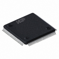
LPC1767FBD100,551 NXP Semiconductors, LPC1767FBD100,551 Datasheet - Page 118

LPC1767FBD100,551
Manufacturer Part Number
LPC1767FBD100,551
Description
IC ARM CORTEX MCU 512K 100-LQFP
Manufacturer
NXP Semiconductors
Series
LPC17xxr
Datasheets
1.LPC1767FBD100551.pdf
(2 pages)
2.LPC1767FBD100551.pdf
(840 pages)
3.LPC1767FBD100551.pdf
(65 pages)
Specifications of LPC1767FBD100,551
Core Processor
ARM® Cortex-M3™
Core Size
32-Bit
Speed
100MHz
Connectivity
Ethernet, I²C, IrDA, Microwire, SPI, SSI, UART/USART
Peripherals
Brown-out Detect/Reset, DMA, I²S, Motor Control PWM, POR, PWM, WDT
Number Of I /o
70
Program Memory Size
512KB (512K x 8)
Program Memory Type
FLASH
Ram Size
64K x 8
Voltage - Supply (vcc/vdd)
2.4 V ~ 3.6 V
Data Converters
A/D 8x12b, D/A 1x10b
Oscillator Type
Internal
Operating Temperature
-40°C ~ 85°C
Package / Case
100-LQFP
Processor Series
LPC17
Core
ARM Cortex M3
3rd Party Development Tools
MDK-ARM, RL-ARM, ULINK2, MCB1760, MCB1760U, MCB1760UME
For Use With
622-1005 - USB IN-CIRCUIT PROG ARM7 LPC2K
Lead Free Status / RoHS Status
Lead free / RoHS Compliant
Eeprom Size
-
Lead Free Status / Rohs Status
Details
Other names
568-4967
935289808551
935289808551
Available stocks
Company
Part Number
Manufacturer
Quantity
Price
Company:
Part Number:
LPC1767FBD100,551
Manufacturer:
NXP Semiconductors
Quantity:
10 000
- Current page: 118 of 840
- Download datasheet (6Mb)
NXP Semiconductors
UM10360
User manual
8.5.19 Open Drain Pin Mode select register 3 (PINMODE_OD3 - 0x4002 C074)
8.5.20 Open Drain Pin Mode select register 4 (PINMODE_OD4 - 0x4002 C078)
Table 96.
[1]
This register controls the open drain mode for Port 3 pins. For details see
mode select register
Table 97.
[1]
This register controls the open drain mode for Port 4 pins. For details see
mode select register
Table 98.
PINMODE
_OD2
5
6
7
8
9
10
11
12
13
31:14
PINMODE
_OD3
24:0
25
26
31:27
PINMODE
_OD4
27:0
Not available on 80-pin package.
Not available on 80-pin package.
Open Drain Pin Mode select register 2 (PINMODE_OD2 - address 0x4002 C070) bit
description
Open Drain Pin Mode select register 3 (PINMODE_OD3 - address 0x4002 C074) bit
description
Open Drain Pin Mode select register 4 (PINMODE_OD4 - address 0x4002 C078) bit
description
Symbol
P2.05OD
P2.06OD
P2.07OD
P2.08OD
P2.09OD
P2.10OD
P2.11OD
P2.12OD
P2.13OD
-
Symbol
-
P3.25OD
P3.26OD
-
Symbol
-
All information provided in this document is subject to legal disclaimers.
[1]
[1]
[1]
[1]
[1]
values”.
values”.
Rev. 2 — 19 August 2010
Value Description
Value Description
0
1
Value Description
Port 2 pin 5 open drain mode control, see P2.00OD
Port 2 pin 6 open drain mode control, see P2.00OD
Port 2 pin 7 open drain mode control, see P2.00OD
Port 2 pin 8 open drain mode control, see P2.00OD
Port 2 pin 9 open drain mode control, see P2.00OD
Port 2 pin 10 open drain mode control, see P2.00OD
Port 2 pin 11 open drain mode control, see P2.00OD
Port 2 pin 12 open drain mode control, see P2.00OD
Port 2 pin 13 open drain mode control, see P2.00OD
Reserved.
Reserved.
Port 3 pin 0 open drain mode control.
P3.25 pin is in the normal (not open drain) mode.
P3.25 pin is in the open drain mode.
Port 3 pin 26 open drain mode control, see P3.25OD
Reserved.
Reserved.
Chapter 8: LPC17xx Pin connect block
UM10360
© NXP B.V. 2010. All rights reserved.
Section 8.4 “Pin
Section 8.4 “Pin
118 of 840
Reset
value
0
0
0
0
0
0
0
0
0
NA
Reset
value
NA
0
0
NA
Reset
value
NA
Related parts for LPC1767FBD100,551
Image
Part Number
Description
Manufacturer
Datasheet
Request
R

Part Number:
Description:
32-bit ARM Cortex-M3 microcontroller; up to 512 kB flash and 64 kB SRAM with Ethernet, USB 2.0 Host/Device/OTG, CAN
Manufacturer:
NXP [NXP Semiconductors]
Datasheet:
Part Number:
Description:
NXP Semiconductors designed the LPC2420/2460 microcontroller around a 16-bit/32-bitARM7TDMI-S CPU core with real-time debug interfaces that include both JTAG andembedded trace
Manufacturer:
NXP Semiconductors
Datasheet:

Part Number:
Description:
NXP Semiconductors designed the LPC2458 microcontroller around a 16-bit/32-bitARM7TDMI-S CPU core with real-time debug interfaces that include both JTAG andembedded trace
Manufacturer:
NXP Semiconductors
Datasheet:
Part Number:
Description:
NXP Semiconductors designed the LPC2468 microcontroller around a 16-bit/32-bitARM7TDMI-S CPU core with real-time debug interfaces that include both JTAG andembedded trace
Manufacturer:
NXP Semiconductors
Datasheet:
Part Number:
Description:
NXP Semiconductors designed the LPC2470 microcontroller, powered by theARM7TDMI-S core, to be a highly integrated microcontroller for a wide range ofapplications that require advanced communications and high quality graphic displays
Manufacturer:
NXP Semiconductors
Datasheet:
Part Number:
Description:
NXP Semiconductors designed the LPC2478 microcontroller, powered by theARM7TDMI-S core, to be a highly integrated microcontroller for a wide range ofapplications that require advanced communications and high quality graphic displays
Manufacturer:
NXP Semiconductors
Datasheet:
Part Number:
Description:
The Philips Semiconductors XA (eXtended Architecture) family of 16-bit single-chip microcontrollers is powerful enough to easily handle the requirements of high performance embedded applications, yet inexpensive enough to compete in the market for hi
Manufacturer:
NXP Semiconductors
Datasheet:
Part Number:
Description:
The XA-S3 device is a member of Philips Semiconductors? XA(eXtended Architecture) family of high performance 16-bitsingle-chip microcontrollers
Manufacturer:
NXP Semiconductors
Datasheet:

Part Number:
Description:
The NXP BlueStreak LH75401/LH75411 family consists of two low-cost 16/32-bit System-on-Chip (SoC) devices
Manufacturer:
NXP Semiconductors
Datasheet:

Part Number:
Description:
The NXP LPC3130/3131 combine an 180 MHz ARM926EJ-S CPU core, high-speed USB2
Manufacturer:
NXP Semiconductors
Datasheet:

Part Number:
Description:
The NXP LPC3141 combine a 270 MHz ARM926EJ-S CPU core, High-speed USB 2
Manufacturer:
NXP Semiconductors

Part Number:
Description:
The NXP LPC3143 combine a 270 MHz ARM926EJ-S CPU core, High-speed USB 2
Manufacturer:
NXP Semiconductors

Part Number:
Description:
The NXP LPC3152 combines an 180 MHz ARM926EJ-S CPU core, High-speed USB 2
Manufacturer:
NXP Semiconductors

Part Number:
Description:
The NXP LPC3154 combines an 180 MHz ARM926EJ-S CPU core, High-speed USB 2
Manufacturer:
NXP Semiconductors


